Continue to Site

Welcome to EDAboard.com

Welcome to our site! EDAboard.com is an international Electronics Discussion Forum focused on EDA software, circuits, schematics, books, theory, papers, asic, pld, 8051, DSP, Network, RF, Analog Design, PCB, Service Manuals... and a whole lot more! To participate you need to register. Registration is free. Click here to register now.

Circuit Board Critique

Status
Not open for further replies.

pigtwo

Member level 4
Member level 4
Joined
Jul 16, 2015
Messages
70
Helped
0
Reputation
0
Reaction score
0
Trophy points
1,286
Activity points
2,771
Hello everyone,

I just finished a circuit board and I am interested in getting a critique of the board/design. This is a personal project but the intention is to use this as example of my work to future employers. I would like to make this as professional looking as possible so if there are things that are not commonly done in professional circuit boards I'd love the know about it so I can correct it.

For context this board has a Spartan 6 with a PROM, SRAM, USB bridge, and ADC attached. The main output is driving a RGB led grid. The highest frequency(besides the USB) is 50 MHz. But few of the signals are driven anywhere close to this. This is my first attempt at really packing the components in as tightly as I could. (One dumb mistake I already noticed is for some reason I used 0805 parts when it was probably unnecessary.)

I've attached(I hope this is allowed) a .zip with the gerber files, a pdf of the schematic(for reference if you want), and the OrCAD .brd file if anyone uses OrCAD.

I welcome and appreciate any comments or recommendations.

Thank you!
 

Attachments

  • LED_GRID_REV_B.zip
    346.1 KB · Views: 122

Hi,

I don't have Orcad.

Klaus
 

I did provide the gerbers also but they can be a little annoying to use(and I'm using the OSHpark naming scheme so the file extensions are weird but they are gerbers.). Maybe I should just post pictures of each layer or the top, bottom, and VCC planes together. I'll try to get some screen shots.

- - - Updated - - -

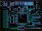
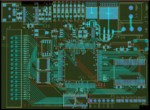
Here are a couple of pictures so no one has to open gerbers for a glance. The first is just the top and bottom layers. The second is the top, bottom and VCC layer. I didn't include the other layer because it is just a ground plane. top_and_bot.PNGtop_vcc_bot.PNG
 

Looks very good to me, including the fatter supply traces which many people forget about.
My only criticism is it has no mounting holes or clear edges that could be used for slot mounting but maybe that is intentional.

Brian.
 

Thank you for the feedback. I'm glad there are no glaring issues. The top of the board was kind of messy so I wasn't sure how much effort should be put into cleaning it up. You're right about the mounting holes. I didn't plan to mount it but I should have include them because every real board would have them.
 

Looks very good to me, including the fatter supply traces which many people forget about.
My only criticism is it has no mounting holes or clear edges that could be used for slot mounting but maybe that is intentional.

Brian.

What about the traces that cross the splits in the Vcc plane? Unless they are slow signals you will see an impedance discontinuity in the traces that cross over the split. If they are high speed you'll end up with signal integrity issues. Most of the boards I've dealt with usually if they run out of planes for Vcc use signal layers to distribute the extra power rails to keep from having signals crossing a split reference plane.
 

What about the traces that cross the splits in the Vcc plane? Unless they are slow signals you will see an impedance discontinuity in the traces that cross over the split. If they are high speed you'll end up with signal integrity issues. Most of the boards I've dealt with usually if they run out of planes for Vcc use signal layers to distribute the extra power rails to keep from having signals crossing a split reference plane.

Thank you for pointing that out. Luckily in this case they are fairly slow signals but I didn't know that crossing power plane divides could cause impedance changes but it's obvious now that you point it out. The problem with doing this is the little gap between the planes will have a difference in the impedance than when the signal is over either of the planes, correct? This sort of leads to a question I've had for a while. On this board the FPGA needs 3.3v and 1.2v. I made that inner power plane the 1.2v plane. How important is it to create a plane like this? I believe only 4 pins need the 1.2v so I easily could have just routed the 1.2v to them thus avoiding the split plane.

Also just out of curiosity, say I have a high speed signal on the top plane, then a unbroken ground plane below that, then a broken VCC plane below that. Would it be ok for the high speed signal to cross over the the broken VCC plane because the ground plane would shield it or could it still have an effect?

Thank you!
 

Your example of a Sig1-Vcc(split)-Gnd-Sig2 with a trace on Sig2 crossing over the split in Vcc plane doesn't change the impedance of that trace on Sig2.

Trace impedance is calculated based on the thickness of the trace, width of the trace, height from the plane (substrate thickness), and the dielectric constant of the substrate. As long as there aren't any splits or gaps in the adjacent plane close to or under the trace the trace impedance won't change. It's one reason for not running high speed signals along the edge of a board right where the edge of the plane ends. If you do that you end up with a high speed trace with poor impedance characteristics, due to the huge air gap on one side of the trace, unless you modify the trace width along that edge.

- - - Updated - - -

Here is a great explanation with far more detail than I provided. https://electronics.stackexchange.com/questions/14262/trace-crossing-splitted-power-plane
 

Ah, that link helped a lot and makes perfect sense. I'm fairly new to signal integrity and so this reminds me of my EMC class where they talked about the return path being just as important as the primary path(terminology?).
 

Your board looks professional at the first glance. I guess it will work fine at 50MHz. Trace impedance will depend also on the geometry of the line (both length and curves and bends) because it will have both inductance and capacitance. Best way to look for poles and zeros in a simulation.
 

That board looks very good, compared to some that we see :)

This is not really a criticism, just me being picky/pedantic - but some of these may help you make it look more pro (not that it needs much).


  1. C1/C3 - are they connected to the red traces that go to U50?
    Could they be moved closer to U50, inside all the traces currently below them.
  2. The red traces that run under BT1, they can all go on top by rotating the resistor to the left of BT1 90 degrees and moving C4 a little.
  3. Your decoupling caps are directly next to their corresponding power pins - yes?
  4. I see no larger reservoir caps on you power rails? might one be req'd here?
  5. What type of switch is SW1? if a vertical toggle switch then I think the on\off labels may be the wrong way around.
  6. Move the tracks away from below Y1, you have the room.
  7. J15v ?? separate the J1 and 5v text a bit more.
  8. The 2 tracks on the top of J4, you only need 1 of those to have 2 vias in, the other can go direct. (unless its a diff pair?)
  9. R20 text is going over a via, check for this in other text - you should not cover a via hole with text as it will be unreadable when the solder mask falls down the hole.
  10. C14 text is obscured by red marks?
    Ditto C16/C16/C18/C19.
    Are these component to component error markers? (I expect so not a problem.)
  11. C25 text is on pads of R40, move it to the right of C25
  12. You have some text reading top to bottom, some text reading bottom to top - make your mind up - what angles should someone be reading it from?
    Always consider the reading angles when the board is in it's environment.
  13. Put U7 text nearer pin 1 - be consistent with the other IC's.
  14. Is the thickness of the text thick enough to print well on the larger font size? Or will it look rather washed out?
  15. As above about mounting features, when you do add them ensure you keep adequate clearance of all copper and components - also consider the tools used to do up screws etc.
  16. I can see several red tracks that have plenty of room to go on the top side for a lot more of their path if not all of it. (a 2nd pair of eyes always picks this up :) )
 
  • Like
Reactions: pigtwo

    pigtwo

    Points: 2
    Helpful Answer Positive Rating
Thank you for the very detailed list! I do appreciate it because I don't really consider it being picky. I try to be very meticulous so things like this would bother me on the finished board if I noticed them. I'll have to start implementing these.
 

Also.... lol

Do those test points all need to be down in the corner?
They are all aerials for the signals and can introduce EMI into the chip so if they do not need to be there and are only used for initial testing then never again, it may be better to have them closer to the pins.

How close to the board edge is the copper? including the inner layer copper there should be a clearance to the board edge, perhaps 0.5mm.
This is to prevent copper edges being on the board edge (that can be shorted to) through manufacturing tolerances.

The schematic, identify each sheet, design name, sheet name, engineer name, date, issue etc.
I can see that the switch is a slide switch so ignore no5 above.
On page 2 you have a few junction points with 4 connections into them, this is bad practice - no more than 3 should be used. Otherwise the dot can fall off and you just have a cross over :)
Net names are under the connections, perhaps this is just the effect of PDF output? if not then they are better not obscured.
The SRAM signals have 3 net name identifiers on, can you disable the middle ones?

U2 pin 2 net has a double >> on it yet the output has nothing? (this applies to lots of other signals too :) )
Again, the testpoints are all in the corner, why not just show them near where they are connected? The reader has to figure out where they go if yo have broken nets like that - where is the other end? do they need to do that?

(This is where you need to look at the schematic and not know what it does, borrow some eyes and see if anything puzzles them or is hard for them to read).

To finish off the design pack for a portfolio:

Draw a manufacturing drawing showing all details for the board build, any requirements and spec for the fabricator.
This prevents the "well you never told us so we did what we wanted" type reply when something is wrong, i.e. the solder resist is too glossy for the placement machine, the board dimension is too small\big etc.

Have coffee.

Draw an "Assembly drawing" showing component positions and all assembly details.
This aids an assembler in what goes where, what direction, what special attention is needed etc. otherwise they may do what they think best because you have not told them different.

Have more coffee.
Basically, the idea of what you want in your head needs communicating to the people that are going to make it for you.

Make a parts list, identify at least 2 suppliers per part, alternatives to show that you have considered the sourcing of components and have not chosen any hat are locked to a single supplier.

Produce Gerbers and Excellon drill file.
Produce ODB++ if you can.

Import both these into a viewer and check they are what they should be to prevent the fabricator making boards that have issues. i.e. a drill size is wrong in the output, the only way to tell is to check it.
(I don't currently have a Gerber viewer installed so cannot look at them).

Have beer. :)
 
  • Like
Reactions: pigtwo

    pigtwo

    Points: 2
    Helpful Answer Positive Rating
I definitely need to fill in the title block info, thank you for reminding me. I was actually going to skip the assembly drawings but honestly its was just out of laziness. Now that you mention it I should make them to complete the project. I do hate making those though.

You're correct about the test point location. I didn't really have a good reason having them there other than the JTAG header is there also. But now that I'm thinking about moving them its obvious I should move them(or the pins) around. Looking at it again I should have changed the pinout of the FPGA to put the ADC, pot, and PROM in the location of the headers. I think I could have cleaned up the top a little by doing that.

I did have a route keep in of 0.5mm(20 mils) but I've just done this out of habit, I didn't really know the reason for it until now.

On page 2 you have a few junction points with 4 connections into them, this is bad practice - no more than 3 should be used. Otherwise the dot can fall off and you just have a cross over :)
Could you explain a little more in detail? I'm not sure what you mean by 'a few junction points with 4 connections'.

As noted the net names being messed up is from the PDF export. I don't know how this happens because I even just print it to PDF so OrCAD shouldn't have to mess with it.

U2 pin 2 net has a double >> on it yet the output has nothing? (this applies to lots of other signals too :) )
Unless I misunderstand, this is because the >> on the net is OrCADs way of saying that the signal connects to somewhere else on another page. While if it doesn't have the >> it connects somewhere on the same page.

I will have to start implementing your comments on the schematic. I'm sort of lazy when it comes to schematics so I really should put some more effort into this one.

Thank you again for the comments. I currently work a job where I do some schematic capture and PCB layout but I'm the only one in the company that does it so I have to teach myself. So I appreciate the direction.
 

Status
Not open for further replies.

Part and Inventory Search

Welcome to EDABoard.com

Sponsor

Back
Top