Continue to Site

Welcome to EDAboard.com

Welcome to our site! EDAboard.com is an international Electronics Discussion Forum focused on EDA software, circuits, schematics, books, theory, papers, asic, pld, 8051, DSP, Network, RF, Analog Design, PCB, Service Manuals... and a whole lot more! To participate you need to register. Registration is free. Click here to register now.

[SOLVED] choosing mosfet and driver

Status
Not open for further replies.

Derun93

Member level 3
Member level 3
Joined
Nov 9, 2015
Messages
60
Helped
0
Reputation
0
Reaction score
0
Trophy points
6
Activity points
532
Hi,
I am planning to use FDS6670A N channel power mosfet. In picture IMosfet, you can see the current waveform on the MOSFET. The first question is if I change my circuit and only the amplitude of the current changes, can the mosfet still conduct? For example, the peak of the current could be 9A or 5A or 500mA. By the way, the link is the datasheet of the MOSFET. Secondly, I am confused about some GATE DRIVER spesifications. I do not know what these spesifications should be. You can find these sepesification in the picture2.
https://www.fairchildsemi.com/datasheets/FD/FDS6670A.pdf
Imosfet.pngspesifications of the driver.png
 

Hi,

wheter a FET is ON or OF is independent of current. It is a question of V_GS.

For sure with a limited V_GS there is a limited current. --> The datasheet will tell you.

***
The current diagram is useless. It just tells, that the current goes form 0A to -9A relatively fast but from -9A to 0A relatively slow. Nobody knows why. Wheter this is good or not. No timing information..

***
You say the specifications of a gate driver is in picture2. But picture shows only a couple of columns with (random) values.

***
We are not here to solve your riddles.
Give complete and detailed informations. Ask dedicated questions.

Then soon you will get satisfying answers.

Klaus
 

First of all, the behavior of the current is determined according to frequency of the circuit. It is true and I just send it to you see the change of the current. For spesificatıon, ı do not what these spesifactıon in the picture means and how can I choose them properly. You can give a range according to MOSFET that I use.
Thank you
Derun

- - - Updated - - -

http://cds.linear.com/docs/en/datasheet/1154fc.pdf
Logic Voltage - VIL, VIH of LTC1154 driver are 0.8V and 2V. Can you tell me please what VIL AND VIH means? are they important parameters to drive FDS6670A N channel power mosfet?
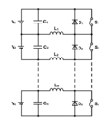
In the picture, switches are going to be MOSFET and assume that 4 lithium ion cells are used.cell balancing.png
 
Last edited:

VIL = Voltage in Low = Low (off) level signal cannot be over 0.8V with respect to ground.
VIH = Voltage in HIgh = High (on) level signal must be over 2V with respect to ground.

r.e. FDS6670A N channel power mosfet... I have no idea, what are VOL and VOH of the LTC1154 driver?
What is VGSth of the FDS6670A at the current your circuit draws?

Come on Derun, read the datasheets a bit more... If you compare these figures from the "electrical characteristics" sections of the respective datasheets, and have fun checking the VGSth graph in the MOSFET datasheet you will find the answers. And quite genuinely, may have doubts based on that information. ...You're not alone. After two hours of reading Op Amp datasheets last night, I am still lost as to what GBW actually can be in real terms r.e. maximum operating frequency :)
 
Thank you for your answers, Mr.d123. Trust me, I am spending so much time by reading datasheets but it is so hard to understand which parameters are crucial for my design. That is why, I am asking questions. One reason is that, I live in Turkey and I am going to order some ICs from abroad and they are really expensive so I have one chance to choose right ICs and order them :) I think I found my driver and MOSFET.
Thank you for your help again.
Derun.
 

The schematic in post #3 reveals a problem that couldn't be guessed from the original question.
In the picture, switches are going to be MOSFET and assume that 4 lithium ion cells are used.
As shown, the post #3 circuit requires the gate drivers source reference for all transistors (except the bottom transistor) to swing over the full battery terminal voltage range. In case of doubt, isolated gate drivers with dc/dc converters or pulse transformers would be required. Usual boot strap drivers are not suited for this application, I think.

Did you analyze expectable waveforms and required driver levels?
What's the controller ground reference?
 

FvM, your reminding is very important. LTC1154 is High Side Micropower MOSFET Driver and can make it.
 
  • Like
Reactions: FvM

    FvM

    Points: 2
    Helpful Answer Positive Rating
LTC1154 is High Side Micropower MOSFET Driver and can make it.
Yes, a similar means like the charge pump incorporated in LTC1154 will be required. The driver speed of this specific device might be insufficient for the application.
 

Status
Not open for further replies.

Similar threads

Part and Inventory Search

Welcome to EDABoard.com

Sponsor

Back
Top