Welcome to our site! EDAboard.com is an international Electronics Discussion Forum focused on EDA software, circuits, schematics, books, theory, papers, asic, pld, 8051, DSP, Network, RF, Analog Design, PCB, Service Manuals... and a whole lot more! To participate you need to register. Registration is free. Click here to register now.
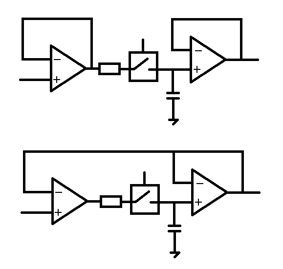
#2 for device drifts, #1 for settling time. Tuning out the switch charge injection to keep #2 from gaining up and then settling from, is an extra design effort I think although some layout-informed switch design attention is always wanted.
#2 is much more critical for the OPAMP. While in #1 both OPAMPS are continously in regulation, in #2 the left OPAMP is continously switched between OPEN_LOOP and CLOSED_LOOP. During OPEN_LOOP the output will saturate at either supply rail and even the input stage may saturate. Then when in CLOSED_LOOP it needs to go the regulated state. Careful OPAMP (circuit) design needs to be done. Especially on
* delay to come out of satuartion
* ringing time and amplitude .. the signal needs to settle within short time
Added:
In both cases the output of the second OPAMP may be used for a guard ring around the capacitor node to reduce leakage current effects. Thus you may reduce the capacitor size, which may give some circuit improvements.
#1 has faster capture time with isolated buffers but may require offset null calibration in fab. and more stable with silicon or NPO caps
#2 has full steps on every sample from either rail from open loop #1 on transition to "sample" and then large dV back to rail on "hold" with instant dV across opening switch and parasitic C feedthru issues but DC input offsets are nulled thus RC time values may need to be raised for fast switches.
Not shown is an alternate dual cap. track and hold and sigma-delta switched C.
There are other topologies for conventional S/H too.
This site uses cookies to help personalise content, tailor your experience and to keep you logged in if you register.
By continuing to use this site, you are consenting to our use of cookies.