haadi20
Full Member level 1

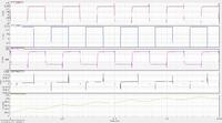
I am simulating a charge pump in C65nm. Icp is 500 uA. The schematic and resulting waveforms are attached.
The questions i have:
1. The up and down currents are not equal, the charging current reaches close to the max current (~484uA) but the discharging current only reaches (~170uA). What needs to be done to make them equal?
2. What could be done to suppress the current spikes at the transition edges?
3. The PMOS have Width of 8.4um and NMOS has width of 6um, doubling the width of PMOS increases the spikes so this is sort of an optimum for minimum spikes. Are the current waveforms and Vtune voltage correct ?
Please answer the above question, thanks in advance.
Points will be awarded to helpful answers.


