Continue to Site

Welcome to EDAboard.com

Welcome to our site! EDAboard.com is an international Electronics Discussion Forum focused on EDA software, circuits, schematics, books, theory, papers, asic, pld, 8051, DSP, Network, RF, Analog Design, PCB, Service Manuals... and a whole lot more! To participate you need to register. Registration is free. Click here to register now.

CGH40010F transistor provided by cree company

Status
Not open for further replies.

Mabrok

Full Member level 4
Full Member level 4
Joined
Mar 1, 2017
Messages
223
Helped
0
Reputation
0
Reaction score
1
Trophy points
18
Activity points
1,597
I have used CGH40010F transistor provided by cree in real fabricated design. during the testing and connecting the DC power supplies to drain and gate terminals. Once I switch on power supply i got short at the drain terminal (circled one in the attached image). Also, drain terminal where i have to connect positive side of the dc power supply, this side connected to the ground when testing with multi meter (test for continuity). This is because the drain terminal and source they are connected when check for continuity (the transistor it self before soldering). So, after soldering the drain side to the circled side highlighted in the attached photo. The whole circled side become ground as the source connected to the ground. please
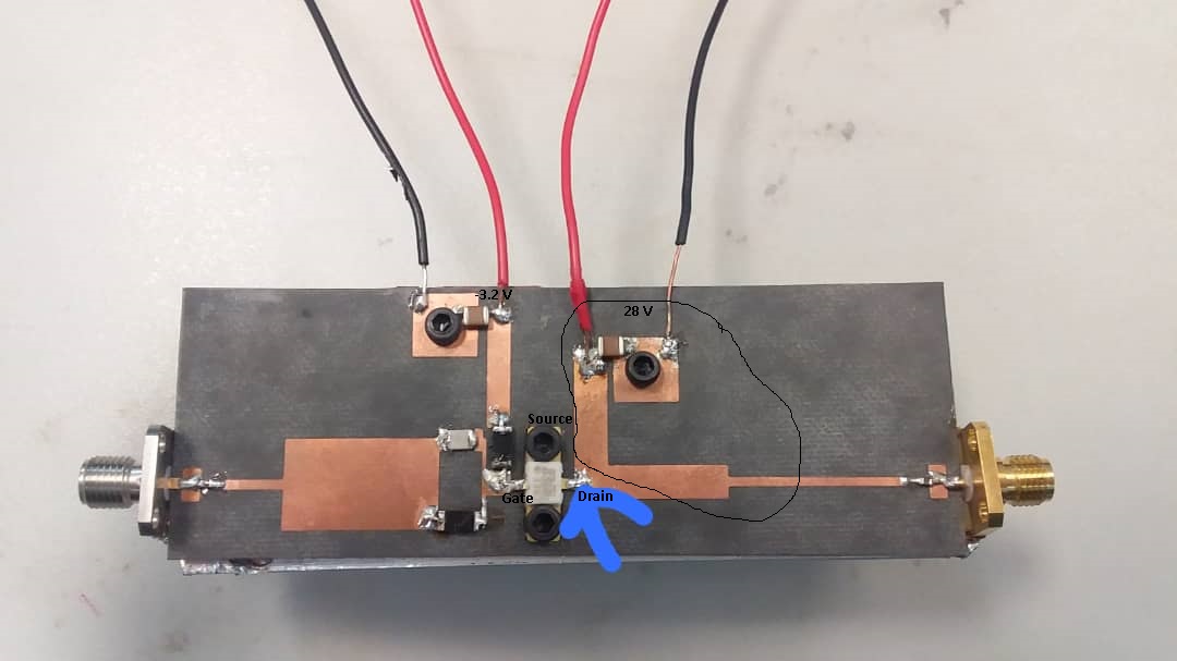
IMG-20200805-WA0012.jpg
advice me about this as this is my first time doing real experiment. Thank you
 

Do you know how to put in order the supply lines in for a Power RFMOS transistor ? If you leave floating the Gate , the Drain will be short circuit to GND..
Search internet to learn this order..
 

    Mabrok

    Points: 2
    Helpful Answer Positive Rating
Do you know how to put in order the supply lines in for a Power RFMOS transistor ? If you leave floating the Gate , the Drain will be short circuit to GND..
Search internet to learn this order..
Thanks for the information. How about this ( drain terminal and source they are connected when check for continuity using multi-meter)?, the transistor itself without any connection to dc power supply
 

The datasheet looks pretty useful. You should read it,
or read it again. This is not a normally-off device.
The channel will pass about an amp at Vgs=0 I'd
say, given that typ -2.7V to choke down to 200mA.
That's going to make your meter beep.

There are good references out there for DC test
methods. What you have is a N channel JFET, all
21st-century-like. If you know what it is that you
want to know, there's a method that you can
follow (given enough combination of equipment
and effort). Poking random pin combinations with
a DMM is hardly ever part of it. But old-timey
methods that need minimal equipment are not
out of the hobbyist / learner's reach - indeed they
are the most basic and useful lesson.


Thanks for the information. How about this ( drain terminal and source they are connected when check for continuity using multi-meter)?, the transistor itself without any connection to dc power supply
When you check Drain-Source while Gate is floating or 0V, you will surely see they are short connected.( why ? find the answer-hint: depletion type )
The true sequence of supplying for this kind of device/system should as follows.
-Connect the Load
-Adjust most minimum level for Vgs( let say -10V) then connect Gate terminal
-Connect Vds
-Connect RF Input without signal
-Adjust quiescent current ( Ids) -for instance 150mA by varying Vgs
-Increase RF level smoothly and observe RF Output

Otherwise the transistor may blow in seconds..
 
  • Like
Reactions: Mabrok

    Mabrok

    Points: 2
    Helpful Answer Positive Rating
When you check Drain-Source while Gate is floating or 0V, you will surely see they are short connected.( why ? find the answer-hint: depletion type )
The true sequence of supplying for this kind of device/system should as follows.
-Connect the Load
-Adjust most minimum level for Vgs( let say -10V) then connect Gate terminal
-Connect Vds
-Connect RF Input without signal
-Adjust quiescent current ( Ids) -for instance 150mA by varying Vgs
-Increase RF level smoothly and observe RF Output

Otherwise the transistor may blow in seconds..
I want to measure S-parameters. So, no input signal applied. I just connect ports (port 1 & 2) from VNA.
 

Wouldn't you prefer to measure S-parameters in
the intended region of operation? This matters.
 

Bias affects capacitance on any port.
Bias affects transconductance. This
is bound to show up in the data.
 

Ok. Then, how to do?
 

I'm a big fan of "test it like you use it".
Match the ports like you would. Bias
it to where the darn datasheet says.

Get your VNA smart guy thing on.
Get your de-embed data "empty
socket" and "shorted socket". Put the
part in and do what you do. Being
sure that it's operating as it would
if you were the guy paying $50 a
pop for them in quantity.
 

I wonder how you arrived at the PCB layout shown in post #1? It seems considerably different to the CGH40010F-AMP evaluation board. Are you sure that the transistor can be operated in your circuit without self-oscillations? They might either kill the transistor or your VNA.
 

When you check Drain-Source while Gate is floating or 0V, you will surely see they are short connected.( why ? find the answer-hint: depletion type )
The true sequence of supplying for this kind of device/system should as follows.
-Connect the Load
-Adjust most minimum level for Vgs( let say -10V) then connect Gate terminal
-Connect Vds
-Connect RF Input without signal
-Adjust quiescent current ( Ids) -for instance 150mA by varying Vgs
-Increase RF level smoothly and observe RF Output

Otherwise the transistor may blow in seconds..
@BigBoss Even with applying negative voltage at the gate side first.then when connect the drain side and try to increase to 28 V. Can not increase, it is shorted to 0V and can not increase any more.
 

So the transistor has got away due to wrong sequence.
When a LDMOS or GaN or similar deplation type Power Transistors are used, the sequence must be as I have written before.
Either Small Signal Measurements or Power Measurements, the correct sequenc should be followed to avoid unwanted accidents.
Because those transistors are very expensive devices.
Means damaged and can not be used?
 

If you try out my suggestion for a simple test
(grounded gate, source resistor) in your other
thread then you would have a pretty good
idea about whether the device is intact.

But following the standard sequencing is
a good idea for this victim, or the next.
 

Means damaged and can not be used?
Unfortunately.. They are very sensitive components even against ESD.
If you leave the gate open so 0 Volt, Ids will be Idss that is pretty high current.Therefore Vgs is adjusted to most permissible negative voltage then Vds is connected and it's adjusted to Idsq by varying Vgs smoothly.Even there is no RF signal at the Input, the transistor may oscillate at this currnet destroys itself in a moment.
 

    Mabrok

    Points: 2
    Helpful Answer Positive Rating
Unfortunately.. They are very sensitive components even against ESD.
If you leave the gate open so 0 Volt, Ids will be Idss that is pretty high current.Therefore Vgs is adjusted to most permissible negative voltage then Vds is connected and it's adjusted to Idsq by varying Vgs smoothly.Even there is no RF signal at the Input, the transistor may oscillate at this currnet destroys itself in a moment.
I never left gate open 0v. At the first time, i applied vgs with -3.2 v and VDS 28 V at the same time (not following the mentioned sequence).
 

I never left gate open 0v. At the first time, i applied vgs with -3.2 v and VDS 28 V at the same time (not following the mentioned sequence).
In this case, ESD has killed your transistor.( my guess )
 

    Mabrok

    Points: 2
    Helpful Answer Positive Rating
In this case, ESD has killed your transistor.( my guess )
Even with using new transistor and following the mentioned sequence by applying negative voltage at the gate side (-5 V), then once connect the drain side is shorted. Can decoupling capacitor made this short?
 

Status
Not open for further replies.

Similar threads

Part and Inventory Search

Welcome to EDABoard.com

Sponsor

Back
Top