Continue to Site

Welcome to EDAboard.com

Welcome to our site! EDAboard.com is an international Electronics Discussion Forum focused on EDA software, circuits, schematics, books, theory, papers, asic, pld, 8051, DSP, Network, RF, Analog Design, PCB, Service Manuals... and a whole lot more! To participate you need to register. Registration is free. Click here to register now.

Center Drills for Pads in Cadsoft eagle

Status
Not open for further replies.

prabhukaran3

Member level 5
Member level 5
Joined
Mar 14, 2013
Messages
93
Helped
2
Reputation
4
Reaction score
2
Trophy points
1,288
Location
Karur
Activity points
2,053
Dear All,.
I am using Cadsoft eagle for simple PCB designs. Recently i have designed my first PCB design in Cadsoft Eagle... everything is ok..
my problem is manufacturer asking "need center dots inside the Pads and Holes to do their jobs without any difficulty... I have tried with drill.aid Ulp.. Its working fine in .brd.. when i do CAM process i can't see the center drills in Solder Layer(inside the pads and holes)
Help Pls.... Cam.centr.pngCenterdrills.png
 

I have never known a manufacturer ask for spot holes, are they drilling by hand!!!
 

Dear Marce,

Your guess is correct.. My Manufacturers are doing manual drilling.. I have seen Films with center dots in pads... Is there any third party tool for placing center drills(dots)?
 

I have never known a manufacturer ask for spot holes, are they drilling by hand!!!
Manufacturers who are doing manual drilling they need center drill in the film.
Follow simple steps....
1.Open your**.brd file.
2.Click on run ULP.
3.Find "drill-aid.ulp".
4.A Center drill diameter Dialogue box opens Enter 0.5 or what ever your manufacturer Demands.
You are done. now you can find center drill layer in layers, then you can export it.
 

Would this have the drill hole in the artwork for the copper layer, that is what is required so the drill centres in the hole and doesn't wander across the pad. This was a standard technique for simple boards that were manually drilled.
 

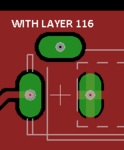
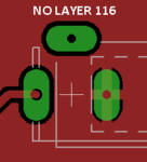
The drill-aid ULP creates uses layer 116 to create the copper fill for holes. The following two images demonstrate (center hole = 0.3 mm):

Capture.PNG Capture1.PNG

If you simply open Eagle and click on layers, you may not see layer 116 as an option. There are also other layers available that do not show by default in the starting dialog. Once you use the ULP, layer 116 appears in the list and can be turned on or off as desired. (As an aside, if you want to erase a drill-aid change, turn off all layers except 116. Then use the highlight and delete dialog.)

The user needs to ensure that whatever is sent to the board manufacturer has layer 116. The manufacturer needs to have it turned on when making its mask for the copper layer.

John
 

you need to run excellon.cam file. so it generate .dll file ,which manufacture can use it for drilling purpose.
 

The manufacturer is manual drilling a drill file is of no use, read the thread.
 

Status
Not open for further replies.

Part and Inventory Search

Welcome to EDABoard.com

Sponsor

Back
Top