Continue to Site

Welcome to EDAboard.com

Welcome to our site! EDAboard.com is an international Electronics Discussion Forum focused on EDA software, circuits, schematics, books, theory, papers, asic, pld, 8051, DSP, Network, RF, Analog Design, PCB, Service Manuals... and a whole lot more! To participate you need to register. Registration is free. Click here to register now.

Capacitance of the ESD protection devices, the bond pad, the bond wire

Status
Not open for further replies.

littlerock

Junior Member level 2
Joined
Mar 13, 2014
Messages
22
Helped
0
Reputation
0
Reaction score
0
Trophy points
1
Activity points
237
Our team is currently working on our final circuit design. We are currently using a 65nm CMOS Technology by TSMC. We wanted to consider the capacitance/parasitics of the ESD protection devices, the bond pad, the bond wire or the interconnection between I/O and analog macro in our schematic simulation. We have tried fabricating an IC before but it failed to function as expected. We suspected that maybe because we were not able to consider such parameters during the schematic simulation. We wanted to do it right this time.

I have read a source, shown below, but it only states about the bond pad parasitics. Is this a reliable source?
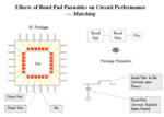

pad.PNG

pad1.PNG

And my question is, how am I supposed to add the parasitics on my circuit schematic and where can I get the values of these components? I will really appreciate any help. Thank you so much.
 

The bond wire has got a series resistance too (it decreases NF) and pin also have some capacitance to ground. Reverse biased ESD diode capacitances are not negligible, add them also to the simulation.
I assume PDK of 65nm process contains the parasitics of the bond wire, the pad is customized sometimes for RF pins, and capacitance is coming from the layout of the pad. Pin capacitance is related to the package, I assume you can find a value somewhere with Google.
And big percent of input capacitance is coming from layout wiring. You should pre-estimate that.
 
We have tried fabricating an IC before but it failed to function as expected. We suspected that maybe because we were not able to consider such parameters during the schematic simulation.
How did you determine that the IC failed to function correctly was due to missing I/O details? It appears from your statement, you haven't definitively determined where the functional fault actually lies. In my past ASIC career, if our team couldn't determine where the fault was we would have been cut loose. Of course all of the ASIC teams I've been on we had 1st pass successful designs due to excellent verification coverage, other groups (the B & C teams) weren't necessarily as fortunate...

Assuming this is a digital ASIC design did you try running the design at a much lower clock frequency to verify that it is functionally correct? If it works at a lower clock frequency then it could be setup/hold issues internal to the device or a problem with I/O timing.

All the ESD protection, bond wire, and bond pad will change is the delay on the input/output signals to/from the die. If you have problems with functionality due to that then you didn't properly constrain the I/O of your design for layout and verify that it met timing.
 

Personally I doubt the parasitics matter to anything with
the possible exception of any dynamic clamps' actuation
time. And that has not to do with parasitics at the pin,
but down the line in the trigger network.

It's a common reaction to try and blame externalities
like models and parasitics, but a little failure analysis
(along with maybe some finer steps in ESD threat
voltage to creep up on the first fail signature, before
catastrophic follow-on events obliterate useful evidence)
would serve you far better than making and chasing
convenient "it's not my design, not my fault" excuses.

If you want to chase CAD related issues I'd start with
the question of whether each pad cell was "blessed" or
"invented", whether every pad-attached device in the
I/O ring has followed ESD design rules, whether current
loops are universally closed at low voltage (ground and
supply domains especially). You might back up and see
whether GGNMOS clamps actually display reasonable
SPICE behaviors and do a full pin-pin nested zap-loop
to show what the weakest pins (i.e. ones that exceed
BVox under threat stimulus) really are, and whether the
loci coincide with the F/A identified fail sites.
 

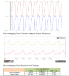
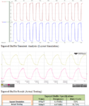
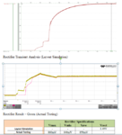
Here's the snapshot of the comparison of the waveform we acquired from the layout simulation and actual or chip testing from the last project. We are working on an indoor light energy harvesting system using a single PV cell (0.5V).

Clock Results (Layout vs Actual/Chip Testing)
Clock Layout vs Actual Result.PNG

Tapered Buffer Results (Layout vs Actual/Chip Testing)
Buffer Layout vs Actual Result.PNG

Rectifier Results (Layout vs Actual/Chip Testing)
Rectifier Layout vs Actual Result.PNG
 

The bond wire has got a series resistance too (it decreases NF) and pin also have some capacitance to ground.

Thanks for the reply frankrose. By the way what does NF means?
 

NF is the noise figure, but I didn't recognize in your project maybe there isn't LNA (low noise amplifier), and you posted actually a LNA. There the parasitics are very important.
Did you simulate the layout with the added measurement equipment's input model? It seems to me something filters out the harmonics from your square wave.
 

And my question is, how am I supposed to add the parasitics on my circuit schematic and where can I get the values of these components? I will really appreciate any help. Thank you so much.

This is one the areas where the tools really svck. There were attempts to do package capture in the tools, but to the best of my knowledge that went nowhere.

For everything that is internal to the chip, the values are well known and given by TSMC. Look at the .lib files provided for the IO cells, all the capacitance values are given. For everything that is external to the chip, you are the one in charge of coming up with a realistic estimation of the (L)RC. The first step would be to contact the company that did the packaging and get their numbers, plug into your simulation, and see if now you match your measurement.
 

Status
Not open for further replies.

Part and Inventory Search

Welcome to EDABoard.com

Sponsor

Back
Top