Continue to Site

Welcome to EDAboard.com

Welcome to our site! EDAboard.com is an international Electronics Discussion Forum focused on EDA software, circuits, schematics, books, theory, papers, asic, pld, 8051, DSP, Network, RF, Analog Design, PCB, Service Manuals... and a whole lot more! To participate you need to register. Registration is free. Click here to register now.

[SOLVED] Can someone explain me why cicruit components are connected like this (see example inside) with hfss dynamic link ?

Status
Not open for further replies.

rdpdo2002

Junior Member level 2
Joined
Oct 28, 2020
Messages
21
Helped
0
Reputation
0
Reaction score
0
Trophy points
1
Activity points
90
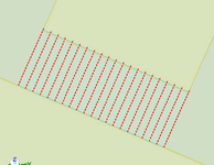
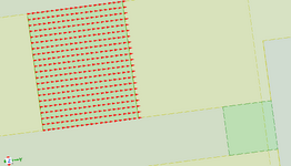
Here is an HFSS - circuit link example : All ports are lumped ports, ZPI defined

1722435445987.png
1722435944883.png


1722436108332.png
1722436220047.png


Connections are made in circuit like this in circuit :

1722435516665.png


For what I understand, the capacitors are well connected but I don't understand how the inductor is connected
because I was expected to get connexions like this :

1722435665240.png


I think it's related to the fact that lumped ports are like current source port, and we have PHI = L*I ?
PErhaps also that the lumped port for the inductance is not connected to any GND ? (like it is for capacitors) ?

Thanks you for your help :)
 

Attachments

  • 1722435845995.png
    1722435845995.png
    47.6 KB · Views: 37
  • 1722435878179.png
    1722435878179.png
    30.2 KB · Views: 35
  • 1722435892121.png
    1722435892121.png
    41.8 KB · Views: 33
  • 1722435907939.png
    1722435907939.png
    89.1 KB · Views: 38

Solution
It looks wrong, but it is correct.

Placing the series element to ground in schematic means: it is connected between the local plus and minus node. That local minus is your terminal on the trace.
It looks wrong, but it is correct.

Placing the series element to ground in schematic means: it is connected between the local plus and minus node. That local minus is your terminal on the trace.
 

    rdpdo2002

    Points: 2
    Helpful Answer Positive Rating
Solution
Thks, ... but well sorry it's not very clear for me :-( ... what you name "minus node" is "local minus" ?? What do you name "terminal on the trace" ? a port ?
 

Your discrete port has 2 terminals, let's call them plus and minus.

STANDARD CASE:
If the "minus" terminals of all ports are connected to the same conductor (let's call that "global ground"), we have the standard situation which is easy to understand. If we short one port in schematic, it means that we have a short across the port. If we connect a 10 Ohm to that port in schematic, we have 10 Ohm between the terminals of that port, which in this standard case means 10 Ohm to global ground.

YOUR CASE WITH LOCAL GROUND:
If the "minus" terminal of your port is connected to some other conductor (other than "global ground"), we still get the impedance across the port that is connected in schematic. If we short the port in schematic to schematic ground, this means we create a short across the port. Note that is NOT a short to global ground now, because your port is floating, with no connection to "global ground".

So, indeed an element connected in schematic to ground will be inserted between the terminals of that port. In your example that means the L is in series, across that ungrounded port.

Hope that makes sense now?
 

Thanks you, I think I have understand...

So all the "0" GND in the circuit schematic are not at the same potential, even if the net name "0" are the same ??

For example, the two "0" GND connected to each capacitors are at same potential (the GND in yellow in HFSS) and the "0" GND wich connect the inductor is at the potential at the "minus" port of the "serie" port, but not at the GND yellow ?

And so there is a "virual" GND port for the "Port1" wich connect to GND yellow also ?

Is it somethong like this ? :

1722543168081.png
 

Yes, that looks ok.

The ground symbol in schematic here does not necessarily mean that all connections are on the same physical net. That would be more obvious if the S-parameter block would provide separate plus and minus terminals for each port. Ports connected to schematic ground are only on the same net if they have a physical connection in the EM model.

BTW, this confusion is seen in other simulators as well. I am not an HFSS user, but have the exact same "floating ground" topic with ADS and other tools.
 

    rdpdo2002

    Points: 2
    Helpful Answer Positive Rating
Status
Not open for further replies.

Part and Inventory Search

Welcome to EDABoard.com

Sponsor

Back
Top