[SOLVED] Cadstar 12.1 outline question
- Thread starter lhavens
- Start date
- Status
- Not open for further replies.

Mattylad
Advanced Member level 3

- Joined
- Sep 7, 2009
- Messages
- 950
- Helped
- 231
- Reputation
- 464
- Reaction score
- 225
- Trophy points
- 1,323
- Location
- Lancashire UK.
- Activity points
- 7,262
You have drawn the outline in copper?
Select the outline and use "duplicate shape" and select "board".
Select the outline and use "duplicate shape" and select "board".
marce
Advanced Member level 5

- Joined
- Feb 23, 2010
- Messages
- 2,103
- Helped
- 630
- Reputation
- 1,263
- Reaction score
- 638
- Trophy points
- 1,393
- Location
- UNITED KINGDOM
- Activity points
- 14,591
I would suggest that if not pressent in assignments Lines add an assignment called board, and use this exclusively as the board outline. Set its initial width to the smallest value your units and decimal places allow.
Mattylad
Advanced Member level 3
- Joined
- Sep 7, 2009
- Messages
- 950
- Helped
- 231
- Reputation
- 464
- Reaction score
- 225
- Trophy points
- 1,323
- Location
- Lancashire UK.
- Activity points
- 7,262
The board outline needs to be drawn as board irrespective of what assignment is used 
marce
Advanced Member level 5
- Joined
- Feb 23, 2010
- Messages
- 2,103
- Helped
- 630
- Reputation
- 1,263
- Reaction score
- 638
- Trophy points
- 1,393
- Location
- UNITED KINGDOM
- Activity points
- 14,591
I never mentioned that, I just gave a tip regarding the fact that having an exclusive assignment for Board outline is good working practice.
lhavens
Junior Member level 2
Sorry people. You may have to have a little patience with me, because I am new to all this. What happen was i imported a dxf. file, and what happened I think is i imported it to the copper layer, but when I started over and reimported it to the board layer it still had a copper outline. I can attach the files if anyone would like to see what i am saying.
So what your saying is i should create a outline for the board on the inside of the copper outline? I will give that a shot.
Thank you everyone I appreciate the input on my troubles.
Lee
So what your saying is i should create a outline for the board on the inside of the copper outline? I will give that a shot.
Thank you everyone I appreciate the input on my troubles.
Lee
marce
Advanced Member level 5
- Joined
- Feb 23, 2010
- Messages
- 2,103
- Helped
- 630
- Reputation
- 1,263
- Reaction score
- 638
- Trophy points
- 1,393
- Location
- UNITED KINGDOM
- Activity points
- 14,591
I would try importing the DXF again. Board outline does not have a specific layer as such, it just is. It is a pre-requisit that all designs require a board outline.
If you create the board outline on the inside of the copper outline then you will be reducing the overall size of the board outline by the width of the copper code used. This is because the copper is drawn as a centre line with half the width either side of this centre line. Thus the actual board outline is the centreline of the copper. Do as Matt says and use duplicate shape, creating a board outline, or turn copper true size of and copy the copper shape, as board usoing the snap features to snap to endpoints. Both methods are worth playing with as they will get you more familiar with some of the drawing fuctions within Cadstar.
If you create the board outline on the inside of the copper outline then you will be reducing the overall size of the board outline by the width of the copper code used. This is because the copper is drawn as a centre line with half the width either side of this centre line. Thus the actual board outline is the centreline of the copper. Do as Matt says and use duplicate shape, creating a board outline, or turn copper true size of and copy the copper shape, as board usoing the snap features to snap to endpoints. Both methods are worth playing with as they will get you more familiar with some of the drawing fuctions within Cadstar.
lhavens
Junior Member level 2
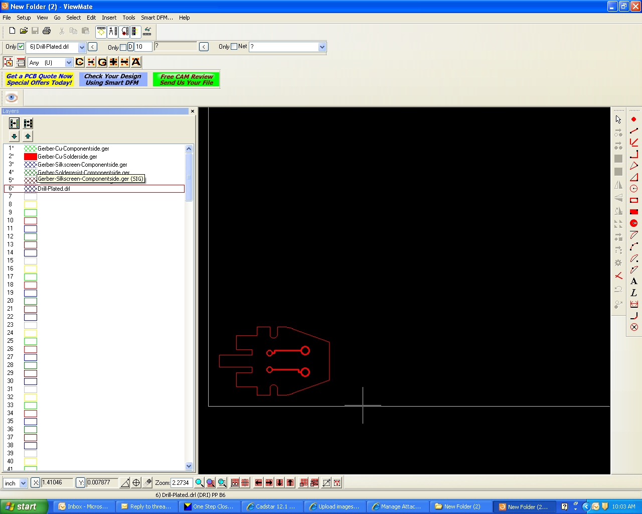
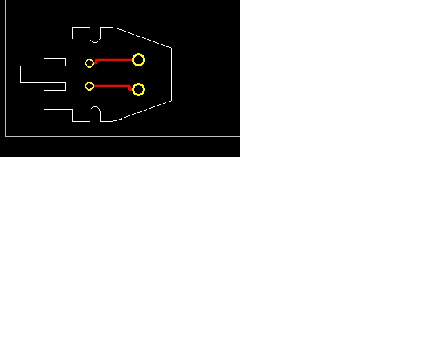
Here are some images to give everyone a better idea of what i am trying to due. I tried duplicating the shape, but it didnt work. First it would not allow me to choose out of the types "Board".
---------- Post added at 10:57 ---------- Previous post was at 10:55 ----------
The picter where it is all red, I just need to get the copper off the outile. But keep the rest of that image.
lhavens
Junior Member level 2
I Have made some it somewhat close to where i want to be. I figured out how to create a duplicate board, and place it on board or template..... etc. The problem is I dont know how to get it to not out line the board in copper. It doesnt out line it in figure and all other components work but there is no outline. I tried fill the shape and it still didnt work.
Mattylad
Advanced Member level 3
- Joined
- Sep 7, 2009
- Messages
- 950
- Helped
- 231
- Reputation
- 464
- Reaction score
- 225
- Trophy points
- 1,323
- Location
- Lancashire UK.
- Activity points
- 7,262
Slightly puzzled by whats happening....
For CADSTAR you are only allowed 1 board outline.
As Marce says - it is best that the board outline has its own line width assignment (so it is not affected by anything else).
When importing - the first page of the mapping file deals with the board, however in the DXF there are some rules to follow.
I.E. no splines, no blocks, the board outline must be on its own layer with nothing else on that layer, the outline must be a single continuous polyline, any cutouts in the board outline in the dxf must be on their own layer (all cutouts on one layer) with nothing else on that layer.
You need to know the names of the layers that the outline and cutouts are on in the dxf, also the units used when creating it - if it is set as unitless then set it as millimetres so the mapping file can match. It is also best of no part of the board oultine is in negative coordinates.
The copper outlines you now have in your design can be deleted.
When importing DXF's it can also help to create some extra layers to import items onto.
If your board outline in the dxf is not a single line, it can be imported as a figure onto a documentation layer instead. Then you can draw a new
board outline using the figure as a reference, using the snap features etc.
---------- Post added at 22:30 ---------- Previous post was at 21:02 ----------
Having looked at the DXF in question, this is indeed in Millimetres, the outline is OK and on its own layer (0).
This imported in easily using the default import options and un selecting the import of components.
The board outline has been changed to use an assignment of Board Outline and sent back to the OP as a PCB with the mapping file.
Although it has no holes or cutouts in.
A bit of a complicated outline, which is why dxf import is so very useful in CADSTAR, took me 60 seconds to import, would take a heck of a lot longer to draw.
marce
Advanced Member level 5
- Joined
- Feb 23, 2010
- Messages
- 2,103
- Helped
- 630
- Reputation
- 1,263
- Reaction score
- 638
- Trophy points
- 1,393
- Location
- UNITED KINGDOM
- Activity points
- 14,591
Interesting, but not an uncommon problem. Personaly I love the DXF inport export function in Cadstar. I can do all the mechanical aspects of the layout (routing (milling), complex board outlines, keep out areas, height restrictions etc), but I have the advantage of having 2D drafting so I can manipulate and control the DXF data, and a £D package, where I can aslo use IDF. Now a lot of what I do with DXF I can do with IDF, but the advantage of using DXF is it is a pretty universal 2D mechanical data interface. It is worth getting to grips with the basics of DXF and how it interfaces with Cadstar, currently DXF 2004 in ascii is the latest version that can be imported reliably, but DXF version R12 (one of the early pre-windows release of Autocad) is a true universal version that any software should be able to import.
For those that want to know a bit more about DXF, have a look around this site:
**broken link removed**
For those that want to know a bit more about DXF, have a look around this site:
**broken link removed**
lhavens
Junior Member level 2
Thank you everyone for taking the time to post to this thread and help out with my issues. I can not thank you enough, it has definitely been extremely helpful. This newbie has learned quite a bit.
- Status
- Not open for further replies.
Similar threads
-
Cadstar library to Altium conversion
- Started by Muthuvel
- Replies: 1
-
Cadstart exporting DXF and cutout into board outline
- Started by Ninja13
- Replies: 2
-
power VIA question
- Started by yefj
- Replies: 1
-
splitting DC bias logic question
- Started by yefj
- Replies: 1