Continue to Site

Welcome to EDAboard.com

Welcome to our site! EDAboard.com is an international Electronics Discussion Forum focused on EDA software, circuits, schematics, books, theory, papers, asic, pld, 8051, DSP, Network, RF, Analog Design, PCB, Service Manuals... and a whole lot more! To participate you need to register. Registration is free. Click here to register now.

Cadence Virtuoso Post-layout simulation using Calibre

presun

Newbie level 5
Newbie level 5
Joined
Jan 15, 2025
Messages
10
Helped
0
Reputation
0
Reaction score
1
Trophy points
3
Activity points
118
Hi I am currently designing a two stage opamp and I am doing post simulation, I have a few questions as I am going through the post simulation.

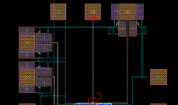
1. even if I apply VDD to the actual pad, the VDD coming into the circuit is bound to have a slight voltage drop, is there any way to check this?
(I have a picture of the layout in the attachment).

2. in post simulation, I would like to see the current flowing through each stage, but I don't know how to do that.
(Currently, I can only measure the current flowing from VDD (sum of the current flowing from 1st and 2nd stage).
 

Attachments

  • asdf.png
    asdf.png
    45 KB · Views: 94
1. The first thing you can do is to measure point-to-point resistance using Calibre PEX RVE and calculate the voltage drop yourself. More complicated approach would be to run IR analysis, and then check the heatmap of the results.
2. I think that the easiest way would be to annotate operating points of your devices (DC or train) by using View -> Annotations after your simulation with extraction is completed.
Hopefully, that helps.
Thank you for your response and I have a few additional questions.

How exactly can I do the IR analysis in #1?

For #2, I tried using the annotations feature but it doesn't seem to work well in config, I was wondering if there is another way.
 
1. For the IR analysis you can use the following tutorial, just choose IR option instead of EM:
2. Instead of config, you can choose .dspf output format in Calibre PEX and then connect it to your simulation housing Setup -> Simulation Files -> Parasitic Files (DSPF). You also should enable Save All for currents and voltages. After your first sim you can note the new names of the currents after extraction and save only the necessary ones.

I think that in general, you are overcomplicating things. As I can see from your screenshot, you have plenty of space for routing - why not to use a wide wire for VDD/ground or even multiple wires? In that case, you won't need to worry about IR drop/ EM compliance at all.

P.S. Please, send me your feedback on the EM/IR tutorial, if something was missing or unclear and I will fix it.
 
1. IR 분석의 경우 다음 튜토리얼을 사용할 수 있습니다. EM 대신 IR 옵션을 선택하기만 하면 됩니다.
[URL 펼쳐보기="true"]https://analoghub.ie/category/cadenceAnalysis/article/cadenceAnalysisEMIR[/URL]
2. config 대신 Calibre PEX에서 .dspf 출력 형식을 선택한 다음 시뮬레이션 하우징 설정 -> 시뮬레이션 파일 -> 기생 파일(DSPF)에 연결할 수 있습니다. 또한 전류 및 전압에 대해 모두 저장을 활성화해야 합니다. 첫 번째 시뮬레이션 후 추출 후 전류의 새 이름을 기록하고 필요한 이름만 저장할 수 있습니다.

일반적으로 당신은 너무 복잡하게 생각하고 있다고 생각합니다. 스크린샷에서 볼 수 있듯이, 라우팅을 위한 충분한 공간이 있습니다. VDD/접지 또는 여러 개의 와이어에 넓은 와이어를 사용하지 않는 이유는 무엇입니까? 그런 경우 IR 드롭/EM 컴플라이언스에 대해 전혀 걱정할 필요가 없습니다.

PS EM/IR 튜토리얼에 대한 피드백을 보내주세요. 누락된 부분이나 불분명한 부분이 있으면 수정하겠습니다.
First of all, thank you for your reply.

In fact, in the actual layout, I added a dummy. I have a layout with the dummy in the attachment.
But even in this version with the dummy added, the voltage was different, so I removed the dummy and was simulating to see where the problem was.
The first photo is the layout with the dummy, and the second photo is the version without the dummy and pads.
(When I ran the post simulation with the layout in the second picture, the results were good, and when I ran the post simulation with the first layout, VOUT,DC was low and the circuit did not behave as I wanted)
1737110728999.png
1737112578162.png

But even in this version with the dummy added, the voltage was different, so I removed the dummy and was simulating to see where the problem was.

1. Is it possible that my dummy design is wrong, the picture of the dummy is also in the attachment.
The blue (odd metal shapes) and yellow (even metal shapes) are shown below.
1737110701132.png
1737110748341.png
1737110765762.png


I have a question during the IR simulation.
1. the conversion of TSMC's IRCX file to EMDATAFILE is not going well.
(I found a guide document from TSMC, but I'm struggling because when I use IRCXTOICT, I actually need the ICT file, unlike the guide document).
 
Last edited:
So, the situation is the following:
  • When you simulated you extracted opamp alone, the results are as expected.
  • When you add dummies + pads, the performance is worse; Also, if you simulate your opamp with pads only, the situation is not improved.
If this is correct, I can suggest the following (let's focus on the difference between extracted opamp and extracted opamp + pads):
1. First of all, let's understand, what exact degradation in performance you are getting: DC gain degradation, BW degradation, offset etc. That will help understanding your problem better; It would be useful to see some of your sim results comparing extracted opamp vs. extracted opamp + pads.
2. Your pads are quite far away from your opamp:
  • Check the width of your power/ground nets - IR drop might cause the degradation (as I mentioned before, simply use Calibre PEX RVE to check the resistance);
  • Check the bias voltages if they are correct;
  • Capacitance of the long nets and pads might affect BW - might cause excessive output loading etc. As a simple test, you can try to add a pad capacitance to the output in parallel with your load and see if it is affecting the performance. You can also check the parasitic capacitance on the output net in RVE and add this capacitance too;
  • I hope that your dummy cells are connected between VDD and ground and not connected to any internal nets. Pay particular attention to the VDD level - I can see that your dummies and opamp are connected to a single VDD wire which might not be able to charge all caps quickly;
  • Regarding the dummy cell design - if it is a custom cell, as soon as you have your DRC/LVS clean on that, it should be ok. I am usually using a custom cell, created from a standard MOM capacitor with some extra layers added, but your design should be fine too.

    3. I also have a few suggestions for your layout in general:
  • If I got the pad names right, your VINN and VINP have very different lengths. Inputs of the opamp should be as symmetrical as possible, routed in parallel with each other (to improve coupling) and preferably close to the input of the circuit:

1.png

  • Same note on the opamp itself - keep VINN and VINP same length (marked in red). I am unsure how you are taking the output, but it looks like you are taking it from the capacitor's plate. This might limit the output current of you amplifier. It's better to place it in the output branch (marked in green);


2.png


  • The differential pair of your opamp doesn't look matched. You should match it by using common centroid technique and surround it with dummy devices;
  • Your critical devices are too close to the well edge (guard rings). You should protect your devices with dummies to avoid WPE and LOD;

    4. Regarding IR drop analysis - it looks like you cannot use ICT file for IR analysis (it is written EM only):
    1737133949004.png

    If you are trying to convert ICT file to emDataFile - you can find the ICT inside some digital design-related folder in PDK. But I think IR analysis is too much for such a simple circuit as yours, it's way easier to debug it by hand and Calibre :) Try to understand what is the exact impact your top level layout has on your circuit and then it would be easier to come up with an idea what might went wrong.
Hopefully, that helps.
 
Last edited:
I see a lot of mention of "different" but I missed
anything quantitative. "Not what I wanted", but
what was that?

If you look close enough everything is "different".
Volts, millivolts, nanovolts. You have to scrub your
results against your "care-abouts" on a quantitative
(if the results aren't so jacked, that it's become a
gross behavioral difference).

If you told me your Vio went out from 659uV to 2mV,
OK, probably something to root out, wrong side
of "round number" spec? Tell me it went to 701uV
and I'd tell you to get a grip.

At design reviews the done thing is a compliance
table, spec vs results and confidence resulting.
Maybe put that out there for context, what's the
beef and why?
More precisely, VOUT,dc has changed.
If the original version without pads and dummies had VOUT,dc=1.5V and the second stage was working fine, the version with pads and dummies has VOUT,dc=500mV, which means that the amplifier is not fulfilling its role.

In addition to VOUT,dc, the voltage at the node where the first stage output goes to the second stage input has also changed from 1.52V -> 1.62V.
 
So, the situation is the following:
  • When you simulated you extracted opamp alone, the results are as expected.
  • When you add dummies + pads, the performance is worse; Also, if you simulate your opamp with pads only, the situation is not improved.
If this is correct, I can suggest the following (let's focus on the difference between extracted opamp and extracted opamp + pads):
1. First of all, let's understand, what exact degradation in performance you are getting: DC gain degradation, BW degradation, offset etc. That will help understanding your problem better; It would be useful to see some of your sim results comparing extracted opamp vs. extracted opamp + pads.
2. Your pads are quite far away from your opamp:
  • Check the width of your power/ground nets - IR drop might cause the degradation (as I mentioned before, simply use Calibre PEX RVE to check the resistance);
  • Check the bias voltages if they are correct;
  • Capacitance of the long nets and pads might affect BW - might cause excessive output loading etc. As a simple test, you can try to add a pad capacitance to the output in parallel with your load and see if it is affecting the performance. You can also check the parasitic capacitance on the output net in RVE and add this capacitance too;
  • I hope that your dummy cells are connected between VDD and ground and not connected to any internal nets. Pay particular attention to the VDD level - I can see that your dummies and opamp are connected to a single VDD wire which might not be able to charge all caps quickly;
  • Regarding the dummy cell design - if it is a custom cell, as soon as you have your DRC/LVS clean on that, it should be ok. I am usually using a custom cell, created from a standard MOM capacitor with some extra layers added, but your design should be fine too.

    3. I also have a few suggestions for your layout in general:
  • If I got the pad names right, your VINN and VINP have very different lengths. Inputs of the opamp should be as symmetrical as possible, routed in parallel with each other (to improve coupling) and preferably close to the input of the circuit:

View attachment 196783
  • Same note on the opamp itself - keep VINN and VINP same length (marked in red). I am unsure how you are taking the output, but it looks like you are taking it from the capacitor's plate. This might limit the output current of you amplifier. It's better to place it in the output branch (marked in green);


View attachment 196784

  • The differential pair of your opamp doesn't look matched. You should match it by using common centroid technique and surround it with dummy devices;
  • Your critical devices are too close to the well edge (guard rings). You should protect your devices with dummies to avoid WPE and LOD;

    4. Regarding IR drop analysis - it looks like you cannot use ICT file for IR analysis (it is written EM only):
    View attachment 196785
    If you are trying to convert ICT file to emDataFile - you can find the ICT inside some digital design-related folder in PDK. But I think IR analysis is too much for such a simple circuit as yours, it's way easier to debug it by hand and Calibre :) Try to understand what is the exact impact your top level layout has on your circuit and then it would be easier to come up with an idea what might went wrong.
Hopefully, that helps.
I've been going over what you've told me and I have one more question.

The picture below is my opamp schematic.
1737180728336.png

I had some problems when designing the following circuit, and I haven't figured out the exact cause yet.
1. in pre-simulation, N5,dc=VOUT1,dc, but in post-simulation, VOUT1,dc came out about 290mV lower than N5,dc. (N5 was the same).
Then, when I did a post-simulation with the dummy and pads attached, the voltage came out a little higher than when I did the simulation without the pads, but still 160mV lower than N5,dc. (Again, N5 was the same as at the beginning.)
(The reason the op amp doesn't work is because the mosfets in the 2nd stage don't saturate as VOUT,dc changes).
I simulated this case by varying VDD and VSS, but the conclusion was that there was no voltage drop from VDD VSS.
(When I tested by changing only VOUT1,dc of the two stage circuit on the schematic, the value of Vout,dc was the same as the post-simulation, so I understood that VDD,VSS has no effect).

The first picture is the result of post-simulating the circuit only, the second is the result of connecting the pads without the dummies, and the third is the result of simulating the circuit with all the dummies added.
1737181309025.png
1737181331212.png
1737181355534.png


Lastly, here is the layout with just the circuit and a little metal added to the VSS side of the layout (width=1um, length=10um) and the post simulation result. (I ran the simulation twice, adjusting the location of the additional metal, In both cases, the RVE resulted in only one additional small capacitor and the parasitic resistive components were unchanged).
1737182489658.png
1737182508840.png

1737183232560.png
1737183278920.png


Have you ever seen a case like this? I keep looking for the cause but haven't found a way...
 
Last edited:
First, your schematic should be debugged before starting the layout. So, my first question will be:
Did you verify your circuit across PVT variations? Does it meet all the specs?

I also don't really understand your approach to debugging either:
1. You provide a lot of node voltages that are meaningless because you have to look at the Vds/Vgs of your devices to see their operating points.
2. You are claiming your sims to be DC whereas I can see the transient simulation with fixed voltages. It is not exactly the same.
3. DC simulations don't reflect the full performance of your opamp, only the operation points of the devices when the small signal is applied to the input. You need to check AC response and transient operation probably (when applying a small-amplitude signal to the input) to understand the performance of the opamp.
4. If you analyse your circuit using DC simulation, it's easier to check by annotating DC operating points to the design by using View -> Annotations -> DC operating points. Annotating DC voltages can be useful as well.
5. If it is your first design, you should probably start by designing more basic circuits (like common source, etc.) and master your design and simulation skills before starting more complex circuits.

1. in pre-simulation, N5,dc=VOUT1,dc, but in post-simulation, VOUT1,dc came out about 290mV lower than N5,dc. (N5 was the same).
Then, when I did a post-simulation with the dummy and pads attached, the voltage came out a little higher than when I did the simulation without the pads, but still 160mV lower than N5,dc.
The reason for that is, most likely, a poor schematic design (some of your devices seems to be balancing on the edge of the operating region (i.e. saturation) and when the resistance of the wire slightly increases, the voltage drop across it causes the device to go out of the desired operation region) + extra parasitic resistance added in layout by the wires between devices.

Lastly, here is the layout with just the circuit and a little metal added to the VSS side of the layout (width=1um, length=10um) and the post simulation result. (I ran the simulation twice, adjusting the location of the additional metal, In both cases, the RVE resulted in only one additional small capacitor and the parasitic resistive components were unchanged).

To answer your question about the layout of the metal wire, it makes complete sense that Calibre adds more parasitic capacitance and not resistance because your metal is connected only to one side. The variation of the VOUT (which I see as the only difference) must be caused by a random settling point of your simulation.
P.S. I think that you need to understand the operation of the 2-stage opamp and basic building blocks better before going with a real design, otherwise we are just trying to catch a black cat in a dark room.


Write your reply...

LaTeX Commands Quick-Menu:

Part and Inventory Search

Welcome to EDABoard.com

Sponsor

Back
Top