rashdriver
Newbie level 5

pcb assembly manufacturer
Dear Friends,
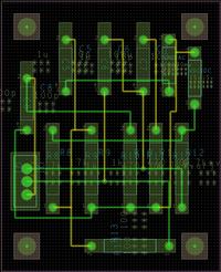
I am new for PCB Editor. I designed a PCB for some project and cross checked the dimension. For conformation i want to make that PCB physically and test the board.
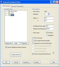
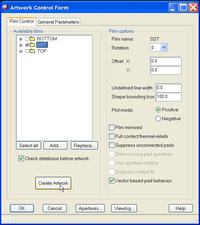
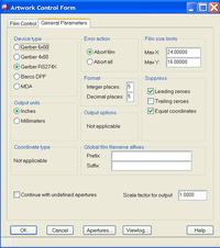
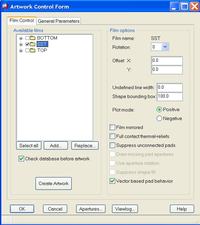
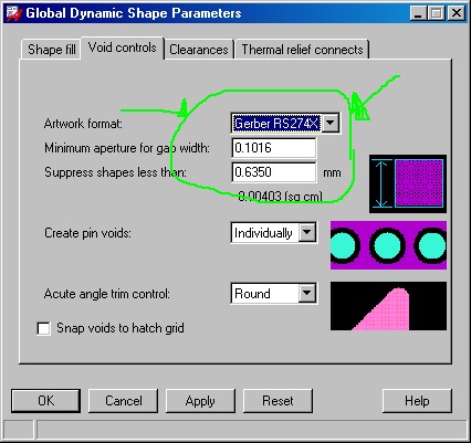
Now i created artwork files for conducting layers.
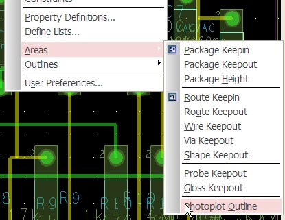
subclass creation, Display match for conducting layer profile then artwork generation.
Now the .art files generated for conducting layers. can i give these files to PCB manufacturer? if no, then what process i should do to get useful file for PCB manufacturing?
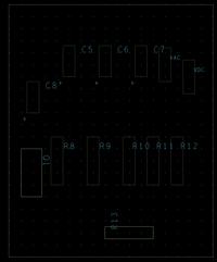
But i dont know how to create mask film, silkscreen film and assembly layout film.
If you give the remaining artwork process with some example 'such as solder mask for avoid soldering in some pads during wave soldering process' that is greatfull for knowing new things and refreshment also.
Kindly help me.
Thanks a lot for all experts.


