Continue to Site

Welcome to EDAboard.com

Welcome to our site! EDAboard.com is an international Electronics Discussion Forum focused on EDA software, circuits, schematics, books, theory, papers, asic, pld, 8051, DSP, Network, RF, Analog Design, PCB, Service Manuals... and a whole lot more! To participate you need to register. Registration is free. Click here to register now.

Cadence layout error !! unbound device !

Status
Not open for further replies.

Ata_sa16

Full Member level 6
Full Member level 6
Joined
Mar 29, 2016
Messages
343
Helped
59
Reputation
118
Reaction score
58
Trophy points
28
Location
Milky Way Galaxy, 179° 56′ 39.4″
Activity points
2,221
Hi guys,

I made a layout of simple inverter in Candece for test. However, there is an error in LVS rule check.

I checked similar thread and I read all but it did not help me.

Anyone knows what is this ???

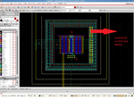
1) Layout

l1.png

2) Error

l2.png

3) Binding rule file

l3.png
 

There is hard to see details in layout, so I can only guess.
1. Check if you have connections from transistors to substrates (bodies).
2. If yes, the technology you are using can be triple well. In this case it is possible do add these diodes (dnwpsub and pndnw) to inverter schematic.
 
There is hard to see details in layout, so I can only guess.
1. Check if you have connections from transistors to substrates (bodies).


Yes this are RF transistors and those square contacts are connected to psub and nwell
l3.png

If yes, the technology you are using can be triple well. In this case it is possible do add these diodes (dnwpsub and pndnw) to inverter schematic.

sounds correct !where should i add these diodes ??
 

You place the symbol from the foundry devices library as
you would any other. Look for the dnwpsub device there
and place it in the schematic with realistic connections
(psub may be a "gimme", or inherited net; nwell is circuit
design defined).

The problem is that extract "sees" the diode and yet it
is not represented within one or both of the explicitly
placed devices' schematic hierarchy. This is a low grade
nuisance in a PDK I'm familiar with, have to place these
diodes in every steenkin' schematic by hand (and then
go back and fiddle each one's properties to match
whatever LVS gripes about next).
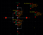


Thank you for your help mate.

But i did not get where should I connect them. I found these 2 diodes in the library.

(psub may be a "gimme", or inherited net; nwell is circuit
design defined) ??!?!?! what is this ?


l4.png
 

I had one case that I had to use not 4-terminal (Drain, Gate, Source, and Body) but 6-terminal transistors (D, G, S, B, and DNW-deep nwell, PSUB- psubstrate). These diodes should be connected between PSUB and DNW - dnwpsub one; and between pwell (body of nmos) and DNW - pwdnw. Probably you have to look into your PDK docummentation to find more information about such transistors. It is also possible that PDK serve some facility with these diodes.
 

dnwpsub diode "plus" or "anode" terminal is the substrate,
gnd! in your schematic. "minus" or "cathode" is the nwell
body terminal of the PMOS.

I am unfamiliar with the triple well process and how you
may be (or not) using dnw. But pwell (if used) would be
the nmos body terminal's net and the "plus"/"anode" of
that other diode; where you connected dnw, I can't ,make
out from the schematic; you'd have to look at the layout
to see how it's tied.
 

Status
Not open for further replies.

Part and Inventory Search

Welcome to EDABoard.com

Sponsor

Back
Top