shaikss
Full Member level 4

Hi,
I am trying to simulate a rectifier with 4-5 number of stages.
I have used pins like RF+, RF- for the +ve and -ve terminals of the RF input and Hi, Lo are the pins for +ve and -ve terminals of the output.
Apart from that, I have used pins like GN+, GN-, GP+, GP- which are used for interconnecting the main and sub blocks.
Now, when I created a block diagram for the first stage, it is throwing warnings that GN-, GN+, GP-, GP+ pins are not being used in symbol.
However, I don't want to use the interconnecting pins reflected in my block diagram.
Shall I ignore these warnings?
What can be done to avoid the warnings?
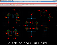
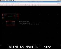
I have attached the schematic of the first stage and its symbol. Please let me know how to avoid this.


