Continue to Site

Welcome to EDAboard.com

Welcome to our site! EDAboard.com is an international Electronics Discussion Forum focused on EDA software, circuits, schematics, books, theory, papers, asic, pld, 8051, DSP, Network, RF, Analog Design, PCB, Service Manuals... and a whole lot more! To participate you need to register. Registration is free. Click here to register now.

Burden Resistor of calculation

Status
Not open for further replies.

nayakajit87

Member level 5
Member level 5
Joined
Aug 13, 2018
Messages
84
Helped
0
Reputation
0
Reaction score
0
Trophy points
6
Activity points
1,065
CT image.png

Dear all,

I am building application for motor protection Relay. I am using Arduino board for interface. I am new to concept of understanding CT calculation. I didnt calculation involved in burden resistor and burden VA .
**broken link removed**

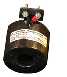
I have attached image of CT which planning to use for application & similarly application circuit used for this application.

How Burden VA is calculated??

how to calculate Burden resistor if i wanted to interface with PIC16F886

How CT size can be reduce? what parameter i need to change to make as per size 2 meet accuracy

if i select this CT , what will be Max current i can supply above which it goes to saturation

what is effect on burden VA , if current exceeds 100A current.
 
Last edited:

The shown 100/5 CT is not well suited for microcontroller application. It must be terminated with a low resistance burden resistor and give respectively low output AC voltage. Maximum output voltage for rated current is 3.75VA/5A=0.75V. Better use a CT like suggested Talema 1030 with low output current and respective higher saturation voltage.
 
  • Like
Reactions: d123

    d123

    Points: 2
    Helpful Answer Positive Rating
How Burden VA is calculated??
ANS:
Burden means resistor connected to output of CT,
VA calculation, when burden resistor connected to output of CT, voltage will appear across the resistor and also current flow through it . This voltage multiplied by current is called VA
how to calculate Burden resistor if i wanted to interface with PIC16F886
ANS:

In this CT the ratio is 100:5 it means 100A applied to primary you will get 5A on output
The CT is big because of 100/5 ratio
Normally for microcontroller interface we use 1000/1 ratio CT


How CT size can be reduce? what parameter i need to change to make as per size 2 meet accuracy
ANS:
Use high ratio 2000:1

if i select this CT , what will be Max current i can supply above which it goes to saturation
ANS:
As per data sheet

what is effect on burden VA , if current exceeds 100A current.
ANS:
We should use burden otherwise CT may saturate
 
  • Like
Reactions: d123

    d123

    Points: 2
    Helpful Answer Positive Rating
Thanks these clarify few doubts of mine. Thats means if i wanted to interface with micro controller . How R1,R2,R3 should be selected.

One thing i understood if i want to communicate with MCU. CT ratio must be 500:1 , 1000:1, 2000:1.
second thing by increasing CT ratio i could reduce the Size

Please let me know How can calculate burden resistor as mentioned image.

Ciruit image.png
 

Hi,

A burden resistor is calculated as any other resistor: using Ohm´s law.

You know the voltages, you know the current, so it´s just R=V/I

Klaus
 

R2, R3, C1 are for biasing purposes. The values are determined by ADC input and leakage currents, 100 ohm isn't a reasonable value. R1 is relevant CT burden. Ipk,secondary should cause slightly below 2.5V voltage drop, so that the ADC input swings between 0 and 5V for maximal input current.
 

I have attached the circuit only for reference. I found most of people using it.
https://talema.com/uploads/documents/product-datasheets/AC%20Series.pdf
In above CT there Burden VA is not mentioned.only told use Burden Resistor and wattage. There might be some equation to find out. some people used R2=R3=100k and R1 as 100ohm

R=V/I – R=2.5/0.042=59.5Ω.
https://www.instructables.com/id/Simple-3-Phase-Arduino-Energy-Meter/

why is considered 42A in above links. can someone explain or gives clarity on hardware topics

- - - Updated - - -

Considering AC1030 data sheet
Ip=30A I max=75A
turns ratio: 1000:1
supply voltage =220vAC
min KW continuous CT can sense =220X30=6.6kw
Max Kw sense for short period=220*75=16.5kw
Irms=1.4*30A=42A

burden resistor= 2.5/(42/1000)=59.5ohm
R1=R2=100kohm Resistor.

Is it correct , what are other care i need to consider while taking hardware design.
 

In above CT there Burden VA is not mentioned
You have linked a short form datasheet only. You get more detailed information about the AC series at Talema internet site. It doesn't give a "VA" number but error percentage versus burden and excitation curves which hold the same information.
 

Here is another datasheet**broken link removed**

There is no VA information
 

Yes, as said. You get all information from the curves and can calculate a VA number if you like.
 

Hi,

Two important things to consider:
* input current, including waveform, frequency,
* ADC input voltage range.

The (convertable) ADC input voltage range is limited. Every signal beyond this range can not be converted, you loose infirmation.
Let's say your ADC is powered with 5V and you use this 5V as reference for the ADC and thus your ADC input voltage range is 0V ... 5V.
Now let's go a bit into details (I didn't read the datasheet, the given values are just examples)

Even for an ideal ADC there is a loss of one LSB in range. For a 10 bit ADC the output range is 0...1023.
The upper limit is 1023. The formula to calculate the voltage from the ADC result usually is: V = V_ref × ADC_value / 1024.
Thus the max decodable value is 5V × 1023 / 1024= 4.995V only.

But this missing 5mV most probably is the least problem.
Every ADC has offet error and gain error.
Let's say the offset error is specified with +/-20mV.
If now the input is 100mV, the ADC may decode it as 100mV -20mV = 80mV .... up to 100mV + 20mV = 120mV.
It results in an error of +/-4LSB.
If the offset is positive you will see every change in analog voltage, but you will never see a ADC_value of "0".
If the offset is negative you can't decode input voltages below this. This means if the offset is -15mV and your ADC_input_voltage is somewhere between 0mV and 15mV --> it can't decode this, the result will always be "0".

Similarily with the gain error, but at the upper end of the input range.
Let's say the ADC gain error is +/--0.5%, then the theoretical upper limit is 4.975V ... 5.025V
Thus the decodable limit may be 4.975V or 4076 LSB (ignoring the offset error)..

But worst will be the VCC error. VCC may have initial deviation from ideal 5V and it may be noisy and drift with load curret, time and temperature...resulting in a huge uncertainty of output value.

Then there additionally are the resistor tolerances and drifts....

All in all I recommend no to go to the limits. Leave some headroom to avoid to get into the decoding limits.
This was the ADC side..
***

Now to the input side:
You say 30A.
But what does this 30A mean?
In ideal case it is 30A RMS of an undistorted, noiseless sinewave.
Then the peak values are +/- 30A x sqrt(2). = +/- 42.43A, a total of 84.85V.

But there will be distortion, there will be noise and there will be increased power_ON current.
A filament light bulb may draw easily 5 times nominal current at startup, a motor will dra a lot higher current at startup, a transformer may draw high peak current when gettin into saturation.

Now you need to decide what peak current you are interested to be decoded. No one can decide this for you.
My recommendation is to leave at least 50% headroom. (Including ADC input headroom)
(But for one of my applications even +/- 5 times the RMS value was not sufficient)

Thus for 30A RMS I'd use 45A RMS input range. Means a total range of 127App.
With a CT ratio of 1000 this means 127mApp at the output side.
This 127mA should become 5V ADC input voltage range: R_burden = V/ I = 5V / 127mA = 39 Ohms

Klaus
 

img2.JPGimg1.JPG

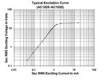
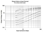
Here are two curve attached for reference. But i could not able to get exact how much volt it will generate if current varied from 0-30A
AC1030 model.

they have mentioned current above 50A effect.

Considering AC1030 data sheet
Ip=30A I max=75A
turns ratio: 1000:1
supply voltage =220vAC
min KW continuous CT can sense =220X30=6.6kw
Max Kw sense for short period=220*75=16.5kw
Irms=1.4*30A=42A

burden resistor= 2.5/(42/1000)=59.5ohm
R1=R2=100kohm Resistor.


If i consider above calculation. What will be Max current applied to arduino pin??
how can i limit current flowing through Analog pin.
 

Status
Not open for further replies.

Similar threads

Part and Inventory Search

Welcome to EDABoard.com

Sponsor

Back
Top