Continue to Site

Welcome to EDAboard.com

Welcome to our site! EDAboard.com is an international Electronics Discussion Forum focused on EDA software, circuits, schematics, books, theory, papers, asic, pld, 8051, DSP, Network, RF, Analog Design, PCB, Service Manuals... and a whole lot more! To participate you need to register. Registration is free. Click here to register now.

Buffer ICs for square wave switching applications

Status
Not open for further replies.

boylesg

Advanced Member level 4
Joined
Jul 15, 2012
Messages
1,023
Helped
5
Reputation
10
Reaction score
6
Trophy points
1,318
Location
Epping, Victoria, Australia
Activity points
11,697
Apart from this 555 based buffer:


What sort of ICs can you use as a buffer in square wave switching applications?

It seems that opamp based buffers, or at least those based on the older opamp designs like LM358AN, are no good.
 

What sort of ICs can you use as a buffer in square wave switching applications?
It depends on the Rise/Fall times of the buffer and its current driving capacity in relation to your design requirements.
Using an opamp may be a good choice for some projects and totally out of the question in other cases.
 

The LM358 is slow because it is old and has low power.

In your application you do not want an ordinary opamp because its output has too much voltage loss. The output high voltage of an LM358 opamp is typically 1.3V less than its supply voltage when its load is only 1mA or less. Its loss is 2V maximum when its output current is 20mA.
An old 741 opamp has more than double the maximum voltage loss of the LM358 at fairly low output currents.
A modern Cmos opamp is "rail-to-rail" (no voltage loss) when its output current is very low.
 

It depends on the Rise/Fall times of the buffer and its current driving capacity in relation to your design requirements.
Using an opamp may be a good choice for some projects and totally out of the question in other cases.

Specifics....

In this case driving a complementary darlington pair emiitter follower with less than 10mA base current and close to rail voltage (15V and 12V during circuit testing) as I can get.

Input is from a CMOS AND gate (15V) - HEF4081.

I tried an LM358AN but I was getting a small triangle wave out of it rather than a nice square waves at the non-inverting input pins.
 

I tried an LM358AN but I was getting a small triangle wave out of it rather than a nice square waves at the non-inverting input pins
Please, post the schematics of the circuit.
 

It all depends on the ESR and load current requirements.

555 can drive so many hundred mA with mV drop which implies the ESR of the driver.
typically 10 Ohms and is related to power handling capability of drivers or RdsOn or Rce of bipolar drivers.

YOu can get as low as 1mOhm ESR on high current half bridges which are complementary MOSFETs. or roll your own with shoot thru prevention by proper bias voltages on complementary drivers.

THere are thousands of drivers in between, so define your specs as I previously stated then the choice is easy. ESR source, load and Voltage swing. Normally for good voltage sourcing, ESR source/load is <1`% for high efficiency or <10% or reasonable. efficiency and poor otherwise.

Next Requirement more relevant in your case is the bandwidth or rise time of the switch and its driver input to generate a rise time < 10% of switch period for ok but < 1% of switch period (min) needed for your application. MOSFETS are typically in the 1uS range. CMOS 74xxxALCV2 can be in the 25 Ohm few nS range like 3V CPU's from ATMEL.. older CMOS rated for 5V and higher tends to be poor BW < ESR ratings, whereas advanced low power <=3V CMOS is much faster and lower driver impedance.. USe the Vol/Iol to determine the ESR rating of the device or the VI curve if avail. Higher the voltage rating, higher the ESR for CMOS in general due to RdsOn, but discrete MOSFETs are better but slower. so your specs matter !!
 

OK, this is what I have soldered.

GDTDriver.jpg

I have not shown the complete schematic (to big for a single screen shot) but this is the relevant part of it. INTERUPTOR 1 is a 20kHz square wave and SQUARE WAVE 1 is about 80kHz.

With the 555 based buffers I have here I got a perfect square wave on my darlington bases.

But then I added those 22nF cap on the 555 outputs, in an attempt to suppress some ringing at the leading edges of the interuptor square wave and it mucked it up.The 555s were overheating too. I assume the impedance of the 22nF caps is to low and working the 555s too hard.

While where at it, what is the correct way to suppress this ringing?
 

I tried an LM358AN but I was getting a small triangle wave out of it rather than a nice square waves.
The old low power LM358 has a very low slew rate. Its datasheet shows a graph that at only about 2kHz its output can swing a triangle wave of only 18V peak-to-peak. At higher frequencies the output cannot slew fast enough so the output triangle wave amplitude is reduced. Isn't your frequency 100kHz?
 

It all depends on the ESR and load current requirements.

555 can drive so many hundred mA with mV drop which implies the ESR of the driver.
typically 10 Ohms and is related to power handling capability of drivers or RdsOn or Rce of bipolar drivers.

YOu can get as low as 1mOhm ESR on high current half bridges which are complementary MOSFETs. or roll your own with shoot thru prevention by proper bias voltages on complementary drivers.

THere are thousands of drivers in between, so define your specs as I previously stated then the choice is easy. ESR source, load and Voltage swing. Normally for good voltage sourcing, ESR source/load is <1`% for high efficiency or <10% or reasonable. efficiency and poor otherwise.

Next Requirement more relevant in your case is the bandwidth or rise time of the switch and its driver input to generate a rise time < 10% of switch period for ok but < 1% of switch period (min) needed for your application. MOSFETS are typically in the 1uS range. CMOS 74xxxALCV2 can be in the 25 Ohm few nS range like 3V CPU's from ATMEL.. older CMOS rated for 5V and higher tends to be poor BW < ESR ratings, whereas advanced low power <=3V CMOS is much faster and lower driver impedance.. USe the Vol/Iol to determine the ESR rating of the device or the VI curve if avail. Higher the voltage rating, higher the ESR for CMOS in general due to RdsOn, but discrete MOSFETs are better but slower. so your specs matter !!

Thanks for that Sunny but the question was more fundamental than that. I don't know what IC names to search for in RS electronics.

I know that HEF and 74HCs are logic gates but I don't know any buffer ICs at all - never used them.

I am actually happy with the 555 based buffer I implemented but I just wanted to look up some dedicated buffer ICs for comparison.
 

First comments, the thread turns out as a continuation of your previous driver thread https://www.edaboard.com/threads/338257/

Using a bipolar 555 output stage as driver isn't particularly effective because you are losing more output swing. Besides discrete transistor circuits that have been already suggested in your previous thread, I would primarly think of gate driver ICs with CMOS output stage, TC427 or similar.
 

Ringing is caused by inductance. Wires all over the place on a solderless breadboard have a lot of inductance because each wire and each strip of contacts is an inductor. Also, your +15V power supply has NO bypass capacitors. The datasheet for an LM555 says that two supply bypass capacitors must be used and connected close to the power supply pins of each 555 or 556.

Why didn't you calculate the reactance of the 22nF capacitors at 80kHz that are shorting the outputs of the 555s? It is only 91 ohms so the peak output current is about 70mA which overheats the 555s and reduces their output voltage swing to about 12V or less.

The datasheet of the LM555 and LM556 shows that with a very low output current its typical output high is 1.3V less than the power supply voltage and is about 1.6V less at 70mA. Its output low goes close to 0V with no load and is typically +0.6V at 70mA.
 

Ringing is caused by inductance. Wires all over the place on a solderless breadboard have a lot of inductance because each wire and each strip of contacts is an inductor. Also, your +15V power supply has NO bypass capacitors. The datasheet for an LM555 says that two supply bypass capacitors must be used and connected close to the power supply pins of each 555 or 556.
Thanks audio - I have never noticed that bit of the 555 datasheet to be honest. Now that I am a little more experienced than I was, I need to start reading the datasheets more thoroughly. At least for the basic components I have a better understanding, although there are still some gaps such as common mode in opamps.


Why didn't you calculate the reactance of the 22nF capacitors at 80kHz that are shorting the outputs of the 555s? It is only 91 ohms so the peak output current is about 70mA which overheats the 555s and reduces their output voltage swing to about 12V or less.

I guess my only excuse is lack of your sort of experience. It seem obvious to me now but when I was mucking around with a simple astable 555 on my breadboard and found a 18nF cap suppressed the ringing......

I might try a 1N4148 to Vcc instead and see if that reduces it a bit.

The datasheet of the LM555 and LM556 shows that with a very low output current its typical output high is 1.3V less than the power supply voltage and is about 1.6V less at 70mA. Its output low goes close to 0V with no load and is typically +0.6V at 70mA.
Well before I put the 22nF cap in, I scoped the bases of my darlingtons and the high of the square wave seemed to be very close to my rail. X10 probe, scale 1V/div => square wave peak was very slightly below the first div. My 12V gel cell was running at about 11.5V, or something like that. I scoped Vcc of my circuit and it was very slightly above the first div.

In my plasma globe circuit I used a complmentary darlington emitter follower pair to run my GDT, but in this case with the the other end of the GDT connected to GND. I also had a 150R resistor on my darlington bases. This circuit worked perfectly so I have added the same 150R resistor to the bases of the darlingtons in this circuit I am working on.

I guess it is just insurance that the base current can never exceed the limits if the darlington transistors.

- - - Updated - - -

First comments, the thread turns out as a continuation of your previous driver thread https://www.edaboard.com/threads/338257/

Using a bipolar 555 output stage as driver isn't particularly effective because you are losing more output swing. Besides discrete transistor circuits that have been already suggested in your previous thread, I would primarly think of gate driver ICs with CMOS output stage, TC427 or similar.

FvM I was using those dedciated FET gate driver ICs but I keep frying them.....and they are expensive.

The pdip UCC27425 I was using is clearly not up to this task because it just kept overheating and I burned one up, The TO.... version of UCC37322 and UC37321 are even more expensive.

With my plasma globe circuit I was using a TO.... version of TC4422 and I burned that up.

So instead of risking another expensive TC4422 I created a complementary darlington emitter follower pair to drive my GDT from GND, and the circuit worked brilliantly and ran my plasma globe.

So I am trying to do the same with my Tesla coil.

Until I gain an understanding what I am doing wrong with these FET gate drive ICs I am not going to use them. I mean they are intended to drive FET gate through a direct connection, as I understand it, rather than through a GDT.

A GDT will have different reluctance characteristics that can go catastrophically bad (for the IC) if you don't completely and thoroughly understand all the issue involved. Or that appears to be the case from my limited experience thus far.

- - - Updated - - -

Your subject line of posts requires a fair amount of detail, i.e. the system wont let you post with only a few words in the subject line.

So every time I come up with a specific question I wish to ask, I put it in a new thread with that detailed question.

Whether or not it is related to the same circuit I am working on.

I assume I am doing the right thing here.

Although I do concede that the threads get mixed up a bit because you guys are reading all of them and not necessarily entirely limiting your answers to the specific question at the top.


Oh and thank you Sunny for your digikey suggestion. From that it appears that I perhaps should be looking for 'line drivers' rather than buffers. In fact I have a salvaged one of those that I could play around with and get to know.
 

So every time I come up with a specific question I wish to ask, I put it in a new thread with that detailed question.

Whether or not it is related to the same circuit I am working on.

I assume I am doing the right thing here.

Although I do concede that the threads get mixed up a bit because you guys are reading all of them and not necessarily entirely limiting your answers to the specific question at the top.

An Edaboard forum rule says:
Duplicates or cross posting are not allowed, avoid creating multiple threads with similar questions, ask all related questions in one thread.

I believe the rule helps Edaboard users to find discussions that answer there questions without browsing countless parallel threads. So please try to follow it.
 

Thankyou audio - I found this in my 555 datasheet:

ADDITIONAL INFORMATION
Adequate power supply bypassing is necessary to
protect associated circuitry. Minimum recommended
is 0.1mF in parallel with 1mF electrolytic.

Very easy to overlook with inexperience but clearly critically important.

Your tip about the decoupling caps has worked a treat in my real circuit - the square waves at my darlington bases are now nice and clean. And their peaks look all but at rail voltage.

But can you explain to me what is going on with the power supply in the circuit that these decoupling caps solve?

- - - Updated - - -

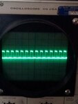
This is what I have at my darlington bases now - a huge improvement.

I removed the 220nF caps and added the two decoupling caps specified in the 555 datasheet, as pointed out by audio.

Waveform.jpg

So that looks a though the peak voltage is probably between 11V and 12V for a 12V gel cell supply. It is a bit hard to be precisely sure with these analog scopes though.

I suppose there will always be a small amount of shoot through current (or what ever you call it) through the darlington pairs in this sort of configuration because it is impossible to get perfect rail to rail output on the bases.

But my TIPs are well heat sinked so they should be OK.
 
Last edited:

I am glad that the decoupling capacitors solved your ringing problem. The wires from the power supply to the 555 ICs and darlingtons are series inductors, especially with the long connecting wires on a solderless breadboard.

Look at the graph of typical output high voltage on the datasheet for the 555. It is 1.3V to 2V less than the power supply voltage because the datasheet shows the output of a 555 is .... guess what? A darlington emitter-follower.
Now you have the voltage losses of two darlingtons in series.
 

Status
Not open for further replies.

Part and Inventory Search

Welcome to EDABoard.com

Sponsor

Back
Top