cupoftea
Advanced Member level 6

Hi,
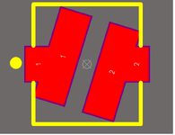
The 74477820 inductor by wurth has a simple footprint in the datasheet
..but in the board we got sent, the footprint is as in the attached...ie, matching the
bottom metalwork, or so it seems.
Which pad pattern is best here?
Its being used in a 20V to 5V Buck
The 74477820 inductor by wurth has a simple footprint in the datasheet
..but in the board we got sent, the footprint is as in the attached...ie, matching the
bottom metalwork, or so it seems.
Which pad pattern is best here?
Its being used in a 20V to 5V Buck