Continue to Site

Welcome to EDAboard.com

Welcome to our site! EDAboard.com is an international Electronics Discussion Forum focused on EDA software, circuits, schematics, books, theory, papers, asic, pld, 8051, DSP, Network, RF, Analog Design, PCB, Service Manuals... and a whole lot more! To participate you need to register. Registration is free. Click here to register now.

Buck Converter Overshoot problem

Status
Not open for further replies.

azadfalah

Full Member level 2
Full Member level 2
Joined
Aug 13, 2016
Messages
145
Helped
1
Reputation
2
Reaction score
2
Trophy points
1,298
Activity points
2,425
Hello friends,

In a asynchronous buck converter
Vin = 50V
Vout = 13V
F = 300khz
Out Current = 500ma

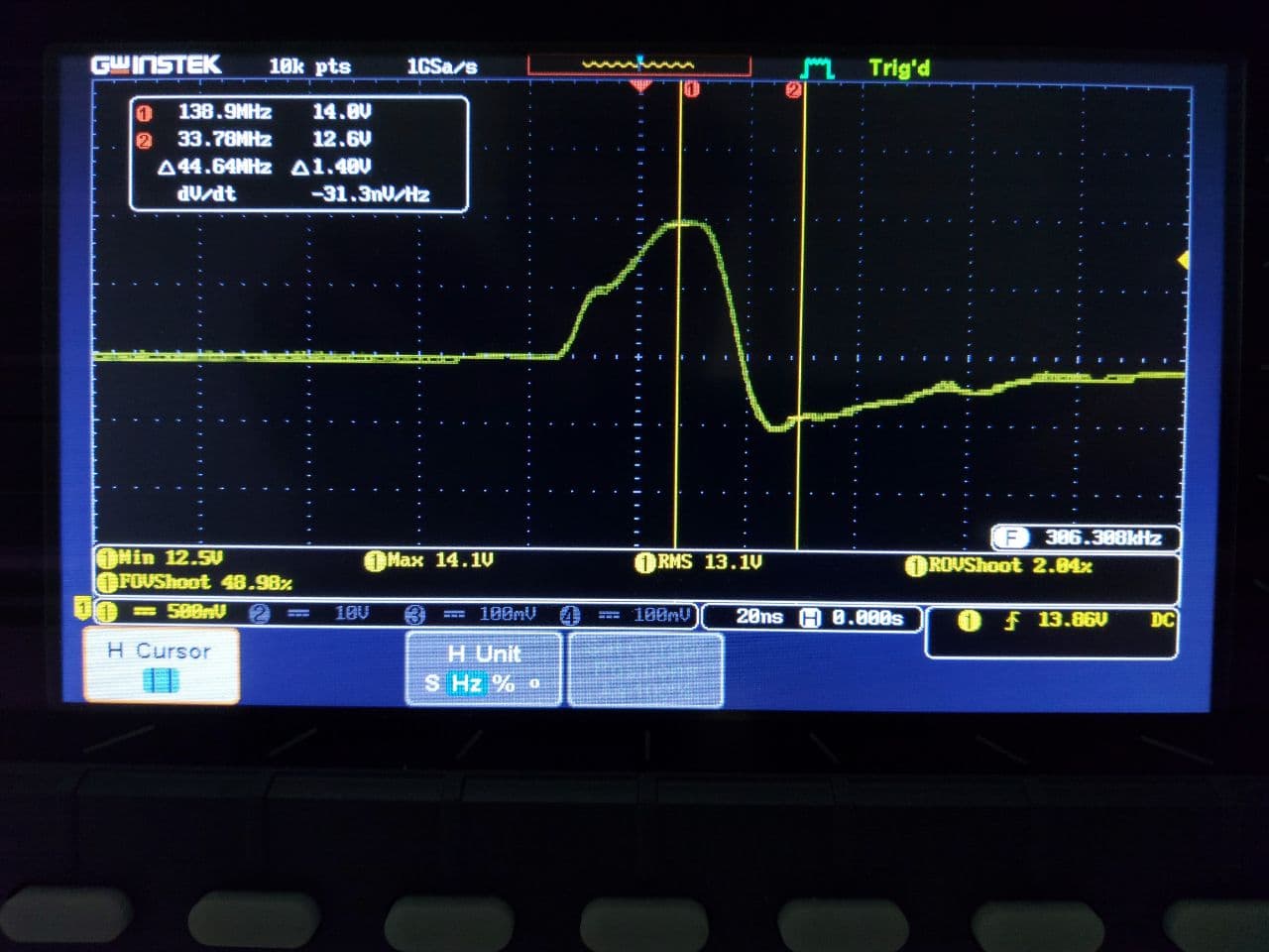
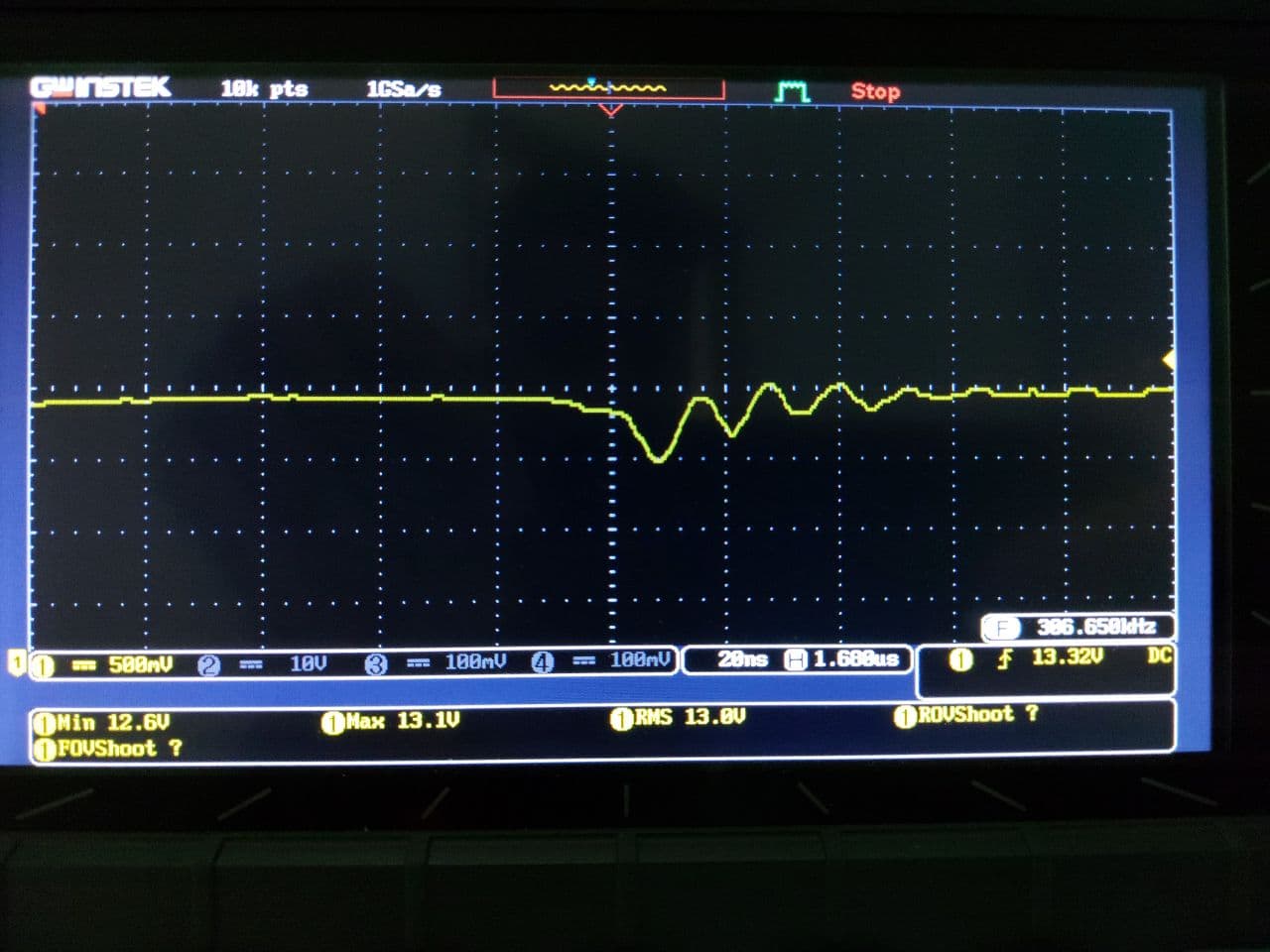
I do not know if this Overshoot is normal?
How can I reduce it?

Output wave
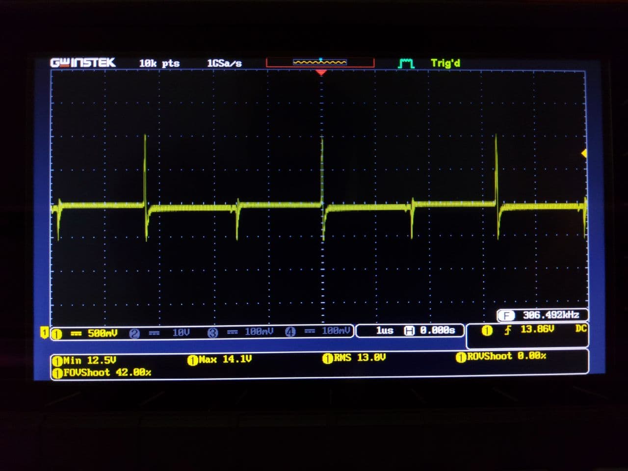
1.jpg


Zoom in overshoot
2.jpg


Zoom in undershoot
3.jpg


Thanks
 

Hi,

I´d say these are switching spikes.
Either a measurement failure or a bad PCB layout.

Klaus
 
Hi,

Don't people place RC or RCD snubbers around transistors and diodes to deal with spikes?
 
Hi,

Don't people place RC or RCD snubbers around transistors and diodes to deal with spikes?

Hi,

Yes, but it is usually rarely used in these cases.
I tested RC snubbers 1nf 10R from phase point to ground
But I could not get a good result
It was almost ineffective
--- Updated ---

Are you using a 10:1 probe with a short ground lead from the probe to the converter ground?


Probe was set to X1 and yes probe ground connected to the converter input ground

(Because the input and output are very close to each other)
 
Last edited:

This is probably a combination of interwinding capacitance
in the output filter inductor (allowing voltage edges to
convert to current spikes) and output filter capacitor ESL
and ESR (failing to absorb those spikes entirely). PCB layout
may add to either, or both.

SW node coupling to round can also produce this by
banging the ground clip, the difference between
VOUT (filter) and GND is all the 'scope displays and
ground can be fairly not-ideal when you've got high
switched circulating currents and input filter
displacement current constantly slapping it upside.

Many supply design pros say you should keep the
ground plane continuous, even under SW trace and
under the inductor, but this seems to be a matter of
how you'd like to receive your beating - output
switching noise itself, output switching noise as an
instigator of other behaviors, or eventual EMC/EMI
qualification failure-redesign cycles. Any of them
can ruin your plan and gain you all the benefits of
enhanced management attention.
 
The problem seemed to be a measurement error there is no noise when I connect the probe to exactly two ends of the load
I mistakenly connected the probe ground to the input terminal ground

However, this noise is present in the input , I designed a simple circuit to learn the buck converter
I feel that if this converter is placed in a compact circuit, the input noise will be problematic and may spread in the circuit.
Please guide me to reduce this noise

A Note: currently the MOSFET driver is IR2103

Simple buck circuit
4.png


Input voltage
5.jpg


Output voltage (After connecting the probe to both ends of the load)
6.jpg


Thanks,
 
Last edited:

Consider that wiring inductance of your PCB is sufficient to create the observed switching noise.

Look at the commutation loop marked in yellow, it comprehends a long ground trace between input capacitor and output diode. A respective voltage transient is induced in this trace by the switched current. With small layout changes, the ground trace can be extended to an almost massive copper pour.

1604741045787.png
 
Hi,

I fully agree with FvM.

And if the big resistor is wire wound... it will kill your Mosfet sooner or later..

The design can't fulfill EMI reqirements ... with unknown effects on devices nearby.

Klaus
 
Consider that wiring inductance of your PCB is sufficient to create the observed switching noise.

Look at the commutation loop marked in yellow, it comprehends a long ground trace between input capacitor and output diode. A respective voltage transient is induced in this trace by the switched current. With small layout changes, the ground trace can be extended to an almost massive copper pour.

View attachment 165476

Thank you for your attention and response

From the beginning resistor is bypassed by a wire

I added a 47uf 50V capacitor at the point near the output diode ground and resistor pad
no more noise at the output but the input waveform is still noisy
Of course, the connection to the input power supply is done with a 2-meter wire


output wave
BuckConverter_Output.jpg


Buck Converter.jpg


input wave

Buck Converter Input.jpg
 

Input spikes can also occur due to capacitor ESL and ESR. Additional ceramic capacitors are advisable.
--- Updated ---

If you want no noise conducted to adjacent modules, additional LC input- and output filters may be necessary. For effective filtering, the switching currents must be kept inside the buck converter.
 
Hi,

I fully agree with FvM.

And if the big resistor is wire wound... it will kill your Mosfet sooner or later..

The design can't fulfill EMI reqirements ... with unknown effects on devices nearby.

Klaus

Hi,

According to the latest Image do you think the EMI situation has improved?
The output voltage of the converter is supply the voltage of the microcontroller by an LDO 3.3V regulator.

Thanks
 

Hi,

why do you think it is improved?
EMI is not a measurement problem. It mainly is a PCB layout problem. But also schematic and part selection problem.
I see no improvement.

Klaus
 
Ah yes - the layout is contributing to the noise seen - some of it will be common mode (CM), which you see when you short the clip and probe tip together and touch gnd or Vout.
Useful to have 1uF film / foil wit short leads from Fet drain to nearest gnd, and the buck diode very close to the choke and gnd return, also a 1uF film foil from diode cathode ( output ) to nearest gnd will help too - good luck ...!
 
Hi,
Friends, do you think there is a problem with this newly designed buck converter PCB?

Buck1.png


Buck2.png

Thanks
 

Sorry, cap from supply to the fet drain to find...
--- Updated ---

... to gnd ...
 
Last edited:

Sorry, cap from supply to the fet drain to find...
--- Updated ---

... to gnd ...

Hi
There are 4 capacitors between the input and ground
The input of the circuit is from the right terminal
 

yup, you need an input ripple current supplying cap directly from the drain to gnd, and then same for the o/p of L1 to gnd - these carry ripple or switching edge current and really reduce volt ripple at switching edges ...
Your large sensing R creates a bigger loop and hence o/p ripple ...
 
yup, you need an input ripple current supplying cap directly from the drain to gnd,

what do you mean ? Are capacitors C5 C1 C6 not enough?
These capacitors are connected directly to the drain and ground
 

Status
Not open for further replies.

Similar threads

Part and Inventory Search

Welcome to EDABoard.com

Sponsor

Back
Top