pragash
Advanced Member level 2

I want to do broadband impedance matching using the negative-image modeling method. I have given all the steps of the negative-image modeling method. my question is on step one as of now but I have given all the steps needed to do broadband impedance matching for an LNA.
The steps to do broadband matching using the negative-image modeling method are:
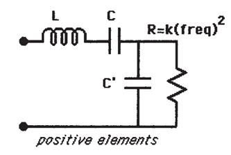
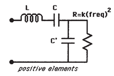
Figure 1: Equivalent component model for transistor input impedances or output impedance across the frequency
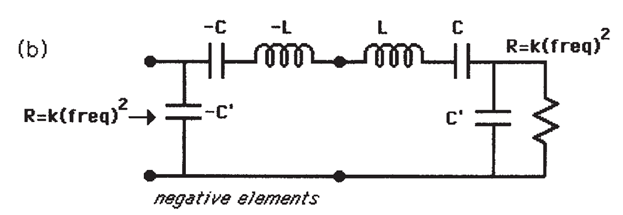
Figure 2: Equivalent component model for transistor input impedances and output impedance across the frequency
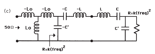
Figure 3: added inductive-T dualizer completes the match to 50;
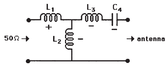
Figure 4: simpler matching structure is shown to work as well as that of Figure 3, where L1 is positive and L2, L3, and C4 are negative;

Figure 5: realizing a negative element with a NIC, where k is positive

Figure 6: structure equivalent to Figure 4, where all elements are positive.
The steps to do broadband matching using the negative-image modeling method are:
- Create an equivalent component model for transistor input impedances and output impedance across the frequency. Assume Figure 1 is an equivalent component model for transistors, either input impedance or output impedance. How can I create an equivalent component model for transistor input and output impedances?
Figure 1: Equivalent component model for transistor input impedances or output impedance across the frequency
- Negative-image modeling begins in Figure 2 by introducing negative elements -L, -C, and -C’ to cancel the corresponding positive parasitic elements L, C, and C_ of the transistor model.
Figure 2: Equivalent component model for transistor input impedances and output impedance across the frequency
- Finally, an inductive-T dualizer completes the non-Foster match in Figure 3.
Figure 3: added inductive-T dualizer completes the match to 50;
- The matching circuit can also be simplified, as shown below;
Figure 4: simpler matching structure is shown to work as well as that of Figure 3, where L1 is positive and L2, L3, and C4 are negative;
- In Figures 1 - 4, the assumption is that individual negative elements are realized by terminating a Negative Impedance Converter (NIC) in the corresponding positive element, as shown in Figure 5.
Figure 5: realizing a negative element with a NIC, where k is positive
- One may alternatively bracket an interconnection of positive elements with NICs to effectively negate that portion of the circuit, as shown in Figure 6.
Figure 6: structure equivalent to Figure 4, where all elements are positive.
