Continue to Site

Welcome to EDAboard.com

Welcome to our site! EDAboard.com is an international Electronics Discussion Forum focused on EDA software, circuits, schematics, books, theory, papers, asic, pld, 8051, DSP, Network, RF, Analog Design, PCB, Service Manuals... and a whole lot more! To participate you need to register. Registration is free. Click here to register now.

Biasing of wide swing current mirror

Status
Not open for further replies.

Junus2012

Advanced Member level 5
Joined
Jan 9, 2012
Messages
1,552
Helped
47
Reputation
98
Reaction score
53
Trophy points
1,328
Location
Italy
Activity points
15,235
Dear friends,

I attached you the picture of the wide swing current mirror and here is my question please,

As I understood from every literature I read that the transistor M5 (by referring to the circuit) has to be four times less than other transistors to get minimum output voltage equal to two saturation currents of M4 and M2 :

Vomin = VDS4 (sat)+VDS2 (sat).

This relationship (M5 = 1/4 M1 = 1/4 M2 = 1/4 M4 = 1/4 M2) is only true if the current in all the branches of this mirror is equal.

Now suppose if we want to mirror the current with different ration from the input, how we will select M5.

Suppose also if we use this mirror in the folded cascoded amplifier for the output cascoded stage where the current in the mirror is varying with the input, again how we will choose the right value of M5

Thank you very much in advance
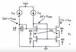
wide swing mirror.jpg
 

This is pretty much theory. When I choose that transistor, I usually set the size by simulation. First, I stack usually 5-6 transistors with the same L as M3 so they can track and for a given current I adjust the widths. I usually leave some margin, say about 50mv for the Vds of M1 above its Vov. Worst case, especially in the diode connected stack M1-M3 is for fast hot corner. It takes a little trial and error but not much.
The battery transistor M5 provides voltage bias, it does not provide current bias as in regular current mirrors. That's why it doesn't matter what currents flow in the cascodes that it biases. What matters is that those cascodes and the currents through them match and are ratioed.
 
Dear Sutpa

Thank you for your kind answer,

when you stack some transistors of M5 it means basically you are dividing the the W/L by the number of your stacked transistors, which the same as given by the picture where he divided it by 4. yes I agree with you by simulation I usually fine tune it,

That was ok when the current of all branches are equal, but still for varying current the biasing voltage of M5 should tracking the change in the current so it change the biasing voltage accordingly, this this I never seen with designers implementing their folded cascode amplifier using the wide swing mirror, they usually give it constant voltage. in this case how they clacuklated the ratio of M5 still not clear to me
 

when you stack some transistors of M5 it means basically you are dividing the the W/L by the number of your stacked transistors, which the same as given by the picture where he divided it by 4.

Not true really... A better way to look at it would be source degeneration, especially for <100nm processes. Because Vth changes with length (and the relationship between Vth and length also has a temperature dependence), I always use the same length for the cascode devices and M5.

Lets say I want to have a 1:10 for input:eek:utput current. In the output size, my cascode will have 10 times the multiplier as my input side cascode transistor. And similarly for the actual current source transistor.

But no, as a designer, I have never biased my cascode with a fixed voltage. It will be hard to maintain bias margins across process and temperature corners.
 
Dear Sutpa

Thank you for your kind answer,

when you stack some transistors of M5 it means basically you are dividing the the W/L by the number of your stacked transistors, which the same as given by the picture where he divided it by 4. yes I agree with you by simulation I usually fine tune it,

That was ok when the current of all branches are equal, but still for varying current the biasing voltage of M5 should tracking the change in the current so it change the biasing voltage accordingly, this this I never seen with designers implementing their folded cascode amplifier using the wide swing mirror, they usually give it constant voltage. in this case how they clacuklated the ratio of M5 still not clear to me


How about something like the attached picture in terms of ratio of transistors. The PMOS stack bias takes a current that's some portion of the main bias current. These stack transistors have the same length Lc as the cascode devices and whatever W that's necessary to produce the gate voltage, say for typical corner or for fast hot corner. The cascode in the bias diode has size of Wc/Lc for a current of 2I. The cascodes in the amplifier have 2x smaller current, so you keep the same Lc for them but divide Wc by 2. Thus all cascode devices work with the same current density. Whatever the corner, the cascodes will track as well as the PMOS stack producing the cascode gate voltage. This gate voltage is not fixed, it tracks the corner. I have seen people do W/5Lc for the cascode bias, but I personally prefer the stack with the same Lc. Mathematically, the ratio is the same, but physically it relies on devices with the same Lc as in the cascode transistors.


cascode_bias.PNG
 
Last edited:
Thank you friends,

I attached you this picture based on your answer which i still please need to confirm about the differences

New Doc 27.jpg

- - - Updated - - -

Note that I am assuming the ideal case of dividing M5
 

If it were not a advanced process node, (1) and (2) would be identical. But in a modern CMOS process, Vth varies with length.
(3) is completely different... You are stacking transistors. Because only your top transistor will be in saturation and the rest in triode, it looks like as if your channel extends across the below 3 devices and is pinched off below the drain of your top transistor. This is really not the case and is just a very first order approximation.
 
Vive thank you for your answer,

nut you now tellling me that the stack is different, however they give the same W/L ration and must provide the same biasing voltage as for solution 1 and 2
 

If you assume the square law, yes indeed. But each of the device will have a different threshold voltage (different bulk-substrate voltages), and this is one of the many effects.
 
Thanks again Viv,

which of the solution in your opinion is better,
as you see the second and the stack solution will consume more area
 

Thanks again Viv,

which of the solution in your opinion is better,
as you see the second and the stack solution will consume more area

If you look at my picture, the stack has the same length as the cascode devices and this is not the case in your picture for solution 3 which defies the purpose of the whole thing. If you stack transistors with the same length as the cascode length, then you end up with effective longer transistor but composed by pieces with the same length. Yes, only top transistor is in saturation and then you have bulk effect but physically or geometrically cascode devices and stacked transistors track each other. The stack, although it is diode connected is not forming a current mirror with the cascodes, it only provides the gate voltage. So my preferred choice will be your solution 3 but with transistor length same as the one in the cascodes. It is in this case similar to solution 2, provided that given the current and the needed gate voltage you can size the bias transistor that provides proper cascode voltage without making W too small.
 
dear suta,
by mistake i make the length to 4 um, it should be the same length 1 um.

What will be the effect if W is smaller,

you can see the difference in area between solution 2 and 3.

thank you once again
 

Usually, there is minimum W you can go down to. Small W in older technology nodes suffers from oxide encroaching under poly, for example or just the limitation of the technology places a limit on the lowest W value. In newer technologies, like 16nm and below you only have certain values of widths that can be used. So, imagine you want to keep the same L as in the cascode devices but you need to keep decreasing the W because you need to go up with the cascode gate bias. And you hit the limit on W. You can either increase the current in the biasing branch or use a stack of transistors, maybe with lower current, reasonable W, same L as in the cascodes and just add enough transistors in series to get the voltage needed.
And I mentioned it several times already, but do simulate fast hot corner and look at the Vov in the diode connected transistors in your mirror like M1-M3 in your picture above. Not sure what technology you use but in that corner the Vgs of M1 is low and will squeeze the Vds of M3 and it may go in triode.
 
How about something like the attached picture in terms of ratio of transistors. The PMOS stack bias takes a current that's some portion of the main bias current. These stack transistors have the same length Lc as the cascode devices and whatever W that's necessary to produce the gate voltage, say for typical corner or for fast hot corner. The cascode in the bias diode has size of Wc/Lc for a current of 2I. The cascodes in the amplifier have 2x smaller current, so you keep the same Lc for them but divide Wc by 2. Thus all cascode devices work with the same current density. Whatever the corner, the cascodes will track as well as the PMOS stack producing the cascode gate voltage. This gate voltage is not fixed, it tracks the corner. I have seen people do W/5Lc for the cascode bias, but I personally prefer the stack with the same Lc. Mathematically, the ratio is the same, but physically it relies on devices with the same Lc as in the cascode transistors.


View attachment 151506
Hi Sutapanaki,
I did try to bias my PMOS wide swing as per your suggestion ( Vov is 200mV), I had few questions
1) How to select the widths of stacked transistors used for biasing ? I kept the lenghts same as that of cascode transistors.
2) How to select the size of cascode transistors in lower node technology like 22nm ? Now I have kept the same size as that of current mirror transistors, but I have read that they have to be smaller.
IMG_20190815_110613__01.jpg
 

Hi Sutapanaki,
I did try to bias my PMOS wide swing as per your suggestion ( Vov is 200mV), I had few questions
1) How to select the widths of stacked transistors used for biasing ? I kept the lenghts same as that of cascode transistors.
2) How to select the size of cascode transistors in lower node technology like 22nm ? Now I have kept the same size as that of current mirror transistors, but I have read that they have to be smaller.
View attachment 154985

1) In your current mirror you design your W/L mirroring transistors with certain Vov in mind, say 200mV. So, whatever voltage you apply at the gates of the cascode transistors (Wc/Lc transistors) it should be enough to define Vds of the mirror devices that's >= Vov. Start with a voltage source connected at the gate of the casodes and vary it until you have good Vds for the mirror transistors in the worst corner. Once you know what gate voltage you need, you can build the stack that biases the cascodes. Choose the current through it and stack transistors, usually 5 or 6 with the same length as the cascodes. Vary the width such that you don't end up building too long of a stack. If you have the same current in the stack as in the diode transistors for the mirror, then just start with the same cascode W as in the mirror.

2) Ususally cascodes are OK with smaller lengths, close to minimum for the technology. Choose W based on the Vov that you need for the cascode transistors or based on the gm of the cascodes, because this will define the non-dominant pole at the source of the cascodes (this is not very important in the case of current mirrors).
----------
a)So, the cascode transitors have to be bigger than current mirrors, so that they have lower Vdsat ?
b)In the above figure, what is the general relation between W/L and Wc/Lc ?
c) The stacked transistors --> Wic/Lc (bias section) in figure, has to be 5 to 6 times smaller with resprct to cascode transistor (Wc/Lc) and not current mirror (W/L), am I right ?
 

It is not necessarily true that the cascode devices are bigger. They can have smaller Lc. Of course smaller the Vov of the cascodes, more headroom you have for mirror transistors. Probably the worst conditions are for the cascode transistor inside the diode side of the mirror. Its drain voltage is limited by the Vgs of the corresponding mirror transistor and it may happen that in extreme corner, like fast hot, the Vgs of the mirror transistor is too small to keep the cascode in saturation. And it is customary to choose cascode Vov based on that. This being said, I don't want to limit myself with giving a general relaton between W/L and Wc/Lc because usually the Lc is different than L.
Yes, the stack transistors relate to Wc/Lc, not W/L.
 
Status
Not open for further replies.

Part and Inventory Search

Welcome to EDABoard.com

Sponsor

Back
Top