Continue to Site

Welcome to EDAboard.com

Welcome to our site! EDAboard.com is an international Electronics Discussion Forum focused on EDA software, circuits, schematics, books, theory, papers, asic, pld, 8051, DSP, Network, RF, Analog Design, PCB, Service Manuals... and a whole lot more! To participate you need to register. Registration is free. Click here to register now.

BGA Power Decaps Routing_ BGA TOP_DECAPS BOTTOM LAYER

Status
Not open for further replies.

tiwari.sachin

Full Member level 6
Full Member level 6
Joined
Aug 1, 2009
Messages
341
Helped
3
Reputation
6
Reaction score
3
Trophy points
1,298
Location
India
Activity points
4,449
I am using a BGA and unable to understand how to route the decaps of power line

Ideally as shown in image below FPGA_3V3 should go to decap first and then to active part (FPGA Power)

Due to space constraints and fan out taken, I have a via between active part and decap and that via connects to FPGA_3V3 and thereby the entire idea of having a decap seems to go for a toss.

Image 3 shows how the decap is connected.


Can anyone suggest me the best way to route the decaps.


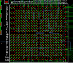
Since there are a lot of them (on FPGA_3V3, FPGA_2V5 and FPGA_1V1), i had planned to keep FPGA on Top layer and Decaps (0402) and bottom. I hardly have a option to use both on same layer.
 

Attachments

  • 1.png
    1.png
    89.9 KB · Views: 221
  • 2.png
    2.png
    102.4 KB · Views: 226
  • 3.png
    3.png
    72.8 KB · Views: 223

The via connecting to the BGA pad should be in the cap pad. It looks like you've got it right. Why do you think this "goes for a toss"? The whole point is that you want the cap provide the little surges of current the BGA pin requires. By keeping trace length, and, therefore, inductance, at a minimum you keep those currents 'local' to the pin.
 

The shown bypass cap routing is the best you can do with standard via technology. Shorter routes and higher wiring density can be achieved with VIPPO (via in pad plated over) technology, but it's more expensive and not necessarily required.
 

The via connecting to the BGA pad should be in the cap pad. It looks like you've got it right. Why do you think this "goes for a toss"? The whole point is that you want the cap provide the little surges of current the BGA pin requires. By keeping trace length, and, therefore, inductance, at a minimum you keep those currents 'local' to the pin.


Attached is the detail of how the routing is. Although the distance is less, the track first connects to the FPGA_3V3 plane and then to the decap which I somehow feel is a wrong way to do. Kindly check and let me know.


I donot have space to take the pins out either
 

Attachments

  • 4.png
    4.png
    24.6 KB · Views: 207

It’s not the wrong way to do it. You need to think about the entire current path and what you are actually trying to accomplish with those caps. See post #2, and read up on decoupling.
 

I didn't need post #4 to know how the routing looks like, it was obvious before. As said, it's the best you can do in the given situation.

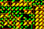
I'm often using similar routing scheme, example below

bga_bypass.PNG

Better alternative is only VIPPO style plugged via

vippo.PNG
 

Thank You. I will keep it as it is. Though I am used to routing it the other way as I was explaining. This time it just got too complex :)
 

Status
Not open for further replies.

Part and Inventory Search

Welcome to EDABoard.com

Sponsor

Back
Top