Continue to Site

Welcome to EDAboard.com

Welcome to our site! EDAboard.com is an international Electronics Discussion Forum focused on EDA software, circuits, schematics, books, theory, papers, asic, pld, 8051, DSP, Network, RF, Analog Design, PCB, Service Manuals... and a whole lot more! To participate you need to register. Registration is free. Click here to register now.

Bandgap strange problem

Status
Not open for further replies.

kickoff1111

Newbie level 6
Newbie level 6
Joined
Dec 16, 2010
Messages
13
Helped
0
Reputation
0
Reaction score
0
Trophy points
1,281
Activity points
1,374
Hi all,
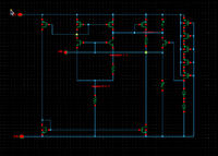
My bandgap circuit is as attached. With a start-up circuit using long channel length PMOS as resistive load and 2 diodes in series.
Now my wafers show low yield in VBG. Good dies show good distribution, but bad dies are all 0V.
Can anyone help me to figure out low yield is due to start-up circuit problem or process variation or others?
I have run all corners in transient and results are all OK, I don't know why.
Need your help.
 

what is the voltage drop across the two diodes in the startup circuitry???
 

what is the voltage drop across the two diodes in the startup circuitry???
The start-up voltage at VBG is 2*VD-VBE. This voltage at VBG will give current to left NPN, hence right NPN.
After loops, the VBG should be steady at around 1.23V.
What I think is in any condition, even there is zero current through BJTs, the VBG should be larger than VBE, why there
are dies whose VBG are stuck at 0V with some percentage around 25%?
Thanks for any help.
 

i think the cap between the VDD and collector of the startup BJT is the problem..i feel that cap pushes the collector node to high impedence state of the startup is not proper.

I did not like the way the cap is connected also since the parasitic node is connected to the collector see that no other parasitics are excited with this
 
Hi rajanarender_suram,
How do you suggest to modify this? If the capacitor is an issue?
Also, will the capacitor be the root cause of low yield?
 

The bandgap circuit seems a little strange to me. I am not shure is that because I miss the basic function or I am stick with standard safe design procedures for bandgaps.

The strange points I found:

1. The inherent kT-loop of the bandgap have a current loop gain defined by the emitter area ratio of the npns. That is typical an integer number. The current gain loop is closed through PMOS mirrors or other feedback topologies. If the current level is below the operating level where both npns in kT-generator the current loop gain is higher than 1. That helps to upwind the current level from startup up to the point where the current gain equals one. At this point the current into the gate of the PMOS driving both bases is zero. What is strange is that if the current is below the level this PMOS is shut off. Typical there is a base on a npn driving with it emitter both bases. That is an inverse loop gain.

2. The npn connected to the two biased series diodes is typical for an initial startup current because the kT-loop gain is below one for very small currents because of leakage and recombinations current. Locking into the gummel plot will show that at low currents the beta drops below one. The startup current lift the initial loop current level above this critical level. What is strange that the startup collector current shunt the kT-loop current instead.

3. The resistor in series with the drain of the driving PMOS does not make sense. The PMOS will act as a current source. A resistor in series with a current source only reduce the voltage headroom.


Please name the devices and possible annotate the op-points.
 

Hi all,
My bandgap circuit is as attached. With a start-up circuit using long channel length PMOS as resistive load and 2 diodes in series.
Now my wafers show low yield in VBG. Good dies show good distribution, but bad dies are all 0V.
Can anyone help me to figure out low yield is due to start-up circuit problem or process variation or others?
I have run all corners in transient and results are all OK, I don't know why.
Need your help.

I think that bad dies are all 0V may refer to start-up circuit problem, once the BGR cannot started up, the output voltage will be 0V. you may need to reconsider about start up circuit.
 

short the collector node of startup BJT to VDD & remove all other connections to the node.
 

Status
Not open for further replies.

Similar threads

Part and Inventory Search

Welcome to EDABoard.com

Sponsor

Back
Top