Continue to Site

Welcome to EDAboard.com

Welcome to our site! EDAboard.com is an international Electronics Discussion Forum focused on EDA software, circuits, schematics, books, theory, papers, asic, pld, 8051, DSP, Network, RF, Analog Design, PCB, Service Manuals... and a whole lot more! To participate you need to register. Registration is free. Click here to register now.

Bandgap Reference Vdc analysis problem! bad results- HELP!

Status
Not open for further replies.

aredhel_vlsi

Member level 4
Member level 4
Joined
Aug 21, 2009
Messages
72
Helped
1
Reputation
2
Reaction score
1
Trophy points
1,288
Activity points
2,013
Hello, I have a problem with a bandgap reference voltage. I have some questions;

1)At a 0.18um technology what voltage reference value should I expect? I tried 1.07 Volt and I think it is ok.

2)My dc temperature analysis is very good, with 0.45 % error at 0-85 celsius values but

what could I do to optimize my V dc analysis ? I manage 15% error which is terrible, I know! any suggestion would be appreciated!

ps; I tried to add some (until 4) diode connected BJT in parallel but I cannot achieve better results. is the number small? do I need a lot more?
 

please show your bandgap schemtic
 

Re: Bandgap Reference Vdc analysis problem! bad results- HEL

Here you are. I'm not in position to design of course, I just found it and try some testings to acquire the results I want..
 

It is ~ 1.2 V typical reference voltage for conventional Bandgap. Try to adjust your circuit to reach this value.

In other words, you should get good Vref vs. Temp characteristic. Typically it obtained at ~1.2 V value of Vref for conventional Bandgap.
 

Re: Bandgap Reference Vdc analysis problem! bad results- HEL

IADanilov said:
It is ~ 1.2 V typical reference voltage for conventional Bandgap. Try to adjust your circuit to reach this value.

In other words, you should get good Vref vs. Temp characteristic. Typically it obtained at ~1.2 V value of Vref for conventional Bandgap.

Well the truth is that my result is far from 1.2 value. At this schematic, I should use a huge a big resistance R2 (on the left) at 1MΩ to achieve that (while R1 =100Ω).Αlso, I need to increase the TP1,2,3,5,6 at 60/2 at least from 52/2, which increases my total current at 500uA at least, and eventually, my consumption..

It is really difficult to change the Vref from 1.092 Volts (which offers me a nice tempco graph) to 1.2 without destroying other parameters. For example at big Vref( ie 1.2V) I have big errors at the temperature analysis too, because I have big W/L of the transistors, and consequently big current. The Vdc also is getting worse at this level!

Also , I think my startup circuit is wrong.

This total topology works nice in low level Vref at 440 mV (I mean tempco and Vdc) . what can I do?
 

Re: Bandgap Reference Vdc analysis problem! bad results- HEL

It depends on technology. Probably, correct Vref is 1.092 V for technology which you use.

Can you show your graphs? (tempco and Vdc)

What are values of R1 and R2?

P.S.
>low level Vref at 440 mV
I think Vref = 440 mV mean that circuit works incorrect.
 

Re: Bandgap Reference Vdc analysis problem! bad results- HEL

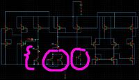
We can't see any sizing information, but presuming
all are "1X", your "diode" (SPNP) ratio of 2:1 is way
low for decent signal to the "op amp". Circled.

Making the output a mirror-fed, independent stack
gives you a degree of freedom but produces no
load-regulation ability at all. OK for capacitors but
not anything that needs DC load range. You can
perhaps modify that stack ({) for a different tempco
than the "core" by varying diode ratio and resistor
value; I'd try and get the core stabilized first, then
"shotgun" some sizings in the output stack to see
what you can get.


Re: Bandgap Reference Vdc analysis problem! bad results- HEL

Make the startup current is zero during the dc analysis when the VREF is up at all temperature and corners. After that, try to tune the Temp Co.
 

Re: Bandgap Reference Vdc analysis problem! bad results- HEL

Hello all, sorry I delayed to answer, I was sick in bed (and a little anxious about all this stuff I 've heard about illness :S).

First, I don't get that; I should have 1.2 V because it is the Eg of the silicon, but there have been bandgap circuits that work at 1.1 or even 1 V.. then why can't I leave it so?

The size of the resistors; R1=178Ω and R2=18kΩ (Ι chose that)

The size of the transistors ;
TN2=10/5 , TN3=10/2, TN1=10/2, TN5=TN4=6.6/2 , TN6=TN7=13/2 (u)
TP2=TP1=TP3=TP5=TP6=52/2, TP7=TP8=26/2, TP4=50u/180n

I know you wonder what the hell is going on with the TP4! I 'll explain..
This schematic is supposed to work at 0.25 um and I try to adjust it at 0.18um.
So, I noticed that I can get a 1 V ref if I change some parameters. The initial sizes were not changed except TP4=2/5(u), TN1=TN3=20/1, TN2=2/5, R2=4kΩ.
I tried to change values and I saw that it depends only if TP4 has such a big W/L which is paradox, I know. it works then as a resistor. Have you got anything to recommend? I know it's also up to BJTs, but if I add more it increases the size of the layout so much! could I do something?

Please do not judge me negatively if this all is wrong, I am a learner ..
My graphs are following. My temp is not posted since I think it is good( 0.45% error for 0-85 C) and ta tan! the Vdc is horrible. I'm desperate!
 

Re: Bandgap Reference Vdc analysis problem! bad results- HEL

dick_freebird said:
We can't see any sizing information, but presuming
all are "1X", your "diode" (SPNP) ratio of 2:1 is way
low for decent signal to the "op amp". Circled.

Yes, I 've seen bandgaps with 8 BJTs in parallel, but this is not good for the layout size. It seems that I can't avoid that, ha? Additionally I tried to simulate with 6 in parallel, and I saw no change at all. I totally agree with you based on the math equations, I just can't see that in practice.

Question; I opened the properties of the BJT and I noticed a parameter "multiplier" by setting that, to 4 means that I have 4 times its value? I don't understand what this is exactly.

dick_freebird said:
Making the output a mirror-fed, independent stack
gives you a degree of freedom but produces no
load-regulation ability at all. OK for capacitors but
not anything that needs DC load range. You can
perhaps modify that stack ({) for a different tempco
than the "core" by varying diode ratio and resistor
value; I'd try and get the core stabilized first, then
"shotgun" some sizings in the output stack to see
what you can get.

the stack includes a BJT and a Resistor. what changes should I do? just trying different values for the resistance? because, as far as I know, I can't add BJTs there.
 

Re: Bandgap Reference Vdc analysis problem! bad results- HEL

well I've tried different values of R2( the left one)

- for R2=18kΩ the error is 0.45% which is satisfying I think but the transient analysis is 1.092 Volt for Vref. it is given first graph.

-for R2=18.5kΩ the error is 0.6% and Vref = 1.099 Volt

-for R2=19kΩ the error is 0.8% , Vref =1.106 volt

as the resistance increases the Vref is better but the Temp graph is getting worse which is natural, but what could I do to compensate that?

what is the % limit error to accept the temp analysis as satisfying one? Is it too wrong to get a 1 Volt V reference?

the graphs are following.
thank you for your support
 

Re: Bandgap Reference Vdc analysis problem! bad results- HEL

Ηi, could somebody tell me how I can get a plot with derivation θVbe/θT using calculator?
Ι have a Vbe graph like the following.. how will I make the deriv expression? I've tried something but it shows the message that it can't be plotted.
 

Re: Bandgap Reference Vdc analysis problem! bad results- HEL

aredhel_vlsi said:
well I've tried different values of R2( the left one)

- for R2=18kΩ the error is 0.45% which is satisfying I think but the transient analysis is 1.092 Volt for Vref. it is given first graph.

-for R2=18.5kΩ the error is 0.6% and Vref = 1.099 Volt

-for R2=19kΩ the error is 0.8% , Vref =1.106 volt

as the resistance increases the Vref is better but the Temp graph is getting worse which is natural, but what could I do to compensate that?

what is the % limit error to accept the temp analysis as satisfying one? Is it too wrong to get a 1 Volt V reference?

the graphs are following.
thank you for your support
A piece of advise to you is to plot the DC analysis graph for temperature.

From your bandgap structure, you should get a Vref of about 1.2V usually, but it can depend on your process. By increasing the value of R2, your Vref temperature coefficient would become more positive. If I were you, I would plot the DC analysis for temperature and adjust R2 until you see a parabola shaped graph for Vref(meaning temperature is compensated). That Vref you get when temperature is compensated would be the bandgap of silicon for your process.
 

Re: Bandgap Reference Vdc analysis problem! bad results- HEL

Hi again! You know, I plotted that dc temperature as you see above. but the problem is that by increasing the value of R, the error of the temp analysis increases, and after some value, Vref becomes 1.7 very briskly. Also, by increasing the values of R the consumption increses too much. When correcting something, something else get worse.

1)Do you know what is the typical consumption of a bandgap in μΑ?
2) What is the limit for the error of temp graph? is 0.6 % good?

Anybody about that question? the help of cadence has not got any example with deriv..

aredhel_vlsi said:
Ηi, could somebody tell me how I can get a plot with derivation θVbe/θT using calculator?
Ι have a Vbe graph like the following.. how will I make the deriv expression? I've tried something but it shows the message that it can't be plotted.
 

Status
Not open for further replies.

Similar threads

Part and Inventory Search

Welcome to EDABoard.com

Sponsor

Back
Top