Continue to Site

Welcome to EDAboard.com

Welcome to our site! EDAboard.com is an international Electronics Discussion Forum focused on EDA software, circuits, schematics, books, theory, papers, asic, pld, 8051, DSP, Network, RF, Analog Design, PCB, Service Manuals... and a whole lot more! To participate you need to register. Registration is free. Click here to register now.

Bandgap architecture doubt

Status
Not open for further replies.

enggan

Member level 1
Member level 1
Joined
Oct 4, 2006
Messages
38
Helped
5
Reputation
10
Reaction score
0
Trophy points
1,286
Activity points
1,527
Hi Friends

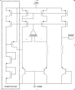
I am designing a bandgap reference circuit in .18um process shown in figgure. my objective is to get a stable output voltage with least temco as possible when i simulated my bandgap i got 1.125v as the voltage which has least temp co but usually 1.25v is the desired bandgap voltage if i set my output voltage to 1.25v my temp co worsens Please help why is this happening.
further i am using the following circuit diagram please suggest the limitations and benifits of this architecture. any suggestions to improve it
43_1320171296.jpg


Thanks and regards
 

this architecture is bad for low voltages. I like it since it is reliable. In your case you probably will have a bit high current through startup circuit - but you can fix it.
Temeperature coefficiant - you can try to play with 1:n ratio. I noticed in my case that if I use usual 1:8 or 16, it does not work well so I went to 132 and made my own bipolar layout. Works great and is flat over temp (well 2mV min to max). You can play with resistors on output since those together with bipolar set your voltage and invluence the temperature dependancy. Use different type or do crazy ser/parallel combinations.
 

@enggan -- the typical bandgap voltage is between 1.2 - 1.3 V. it is not defined to be 1.25V. the theoretical value for silicon is 1.22eV at 0K. u can select the value which gives u least tempco. the tempco is based on a number of factors as teddy explained. it might be difficult to stack 2 pmos in 0.18um process with 1.8V supply. but the basic architecture is solid.
 

Hi Friends

Thanks for your reply I forgot to mention that though my process is 0.18um but I have got supply voltage of 3.3v (these are high voltage mosfets) sorry for that, so stacking of two mosfets is not a problem in my case but as teddy mentioned this is a bad architecture for low voltages does it still apply in my case with supply voltage of 3.3v.

I have used bjt ratio of 4:32 should I increase this ratio, actually I have read in some literature that we should not use 1:n but instead m:n reason I don't know?
I have simulated this architecture for temp. range of -40 to 125 and my temp co varies from 19 to 70 ppm/oc over various process corners i havent included my mismatches yet is this much variation ok

Thanks and regards
 

Hi Friends

Thanks for your reply I forgot to mention that though my process is 0.18um but I have got supply voltage of 3.3v (these are high voltage mosfets) sorry for that, so stacking of two mosfets is not a problem in my case but as teddy mentioned this is a bad architecture for low voltages does it still apply in my case with supply voltage of 3.3v.

if u are having 3.3v and high voltage devices, this is a good architecture.

I have used bjt ratio of 4:32 should I increase this ratio, actually I have read in some literature that we should not use 1:n but instead m:n reason I don't know?
I have simulated this architecture for temp. range of -40 to 125 and my temp co varies from 19 to 70 ppm/oc over various process corners i havent included my mismatches yet is this much variation ok

Thanks and regards

Using m:n instead of 1:n is due to two reasons.
1) in 1:n you have a higher mismatch due to single device and more chances of failure and reliability issues
2) also when you have large currents in the branches you need more diode area to maintain linearity. (plot I-V curves and try to operate in the linear region)

the linearity will affect your tempco. to obtain flat tempco, you can also try fancy resistor combination tricks to cancel out tempco variations.
 
Before using the ratio m:n or 1:n, check with the technologies available.
In layout, commom centroid method is used for BJT. It will give good matching. But it supports 1:4 1:8 1:16.
amomg these 1:8 will give good results.
 

The npns in your schematic are backwards so it is going to do something weird. Other than that, there is nothing wrong with the topology.

1.125 V seems a little low. If properly designed, the "magic" voltage should not depend the the bipolar ration (1:8 or 1:16, etc). It will, however, depend on the temp-co of the resistor. If it isn't that, there is probably something wrong in your circuit. Things that could affect the results:
1) The mirror ratio of the rightmost and 2nd from the rightmost PMOS devices is not EXACTLY 1.
2) Your startup circuit isn't shutting completely off.
3) Your bipolars are biased at too high or too low a current density.

Your Vout vs temp curve should be parabolic with the voltages at -55 and 125C about 4 mV lower than the value at 30C. If it looks different you probably have something biased incorrectly. If you can't figure it out, post the Vout vs Temp curve and how much current you have in each leg.
 

If properly designed, the "magic" voltage should not depend the the bipolar ration (1:8 or 1:16, etc). It will, however, depend on the temp-co of the resistor.

how would you arrive at this "magic" voltage for a given process. just from simulations ?
 

If the models are good enough you can find the "magic voltage" with simulation, but usually you need to have measured data. Really what you are trying to find is the proper combination of resistor and bipolar ratios and current density in the bipolar to put the zero-TC portion where you want it.

---------- Post added at 16:17 ---------- Previous post was at 15:38 ----------

The more I think about it, the more my first guess would be mismatch from finite output resistance in the pair on the right. You can correct this by putting a resistor in the middle leg (above the resistor that is already there) like the circuit on the right below. This will match the voltage seen by both devices in the mirror. In your circuit you would mirror and replicate the voltage instead of taking it on the right side.
RinconMora_Fig2.gif

(ref **broken link removed**).


If you are going to use an opamp, I personally prefer this topology.
Image1508.gif


(ref EDACafe: Power, accuracy and noise aspects in CMOS mixed-signal design)

It has lower noise since it uses resistors to mirror the current. It can also source current.

Consider labeling your devices when you post a schematic as it will be easier to discuss your circuit.

rg
 
Last edited:

Status
Not open for further replies.

Part and Inventory Search

Welcome to EDABoard.com

Sponsor

Back
Top