Tusharsinh
Newbie level 4

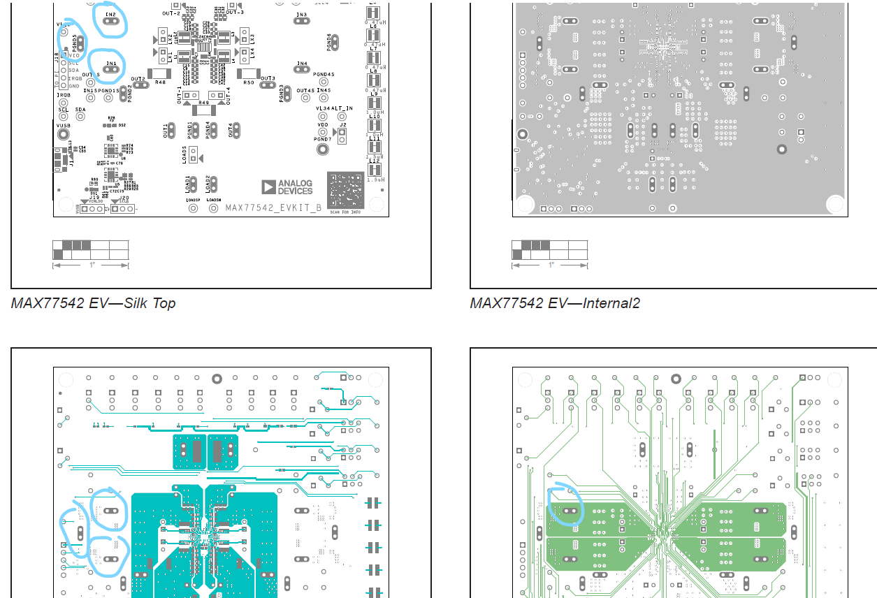
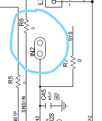
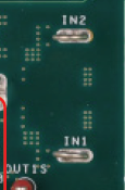
I am studying max77542ev kit pdf. In which I am not getting some of the footprints. In BOM, It suggests that In1 - In 4 etc. are buss bar (20 gauge copper wire which looks sorted in pcb board image). In PCB layout some of that are directly connected to polygon (see in pcb layout image right bottom layer in this case). What are this ? It neither seems like test points neither jumper. What is the purpose of this? Why silk screen in that area is directly exposed to copper pads?


