Continue to Site

Welcome to EDAboard.com

Welcome to our site! EDAboard.com is an international Electronics Discussion Forum focused on EDA software, circuits, schematics, books, theory, papers, asic, pld, 8051, DSP, Network, RF, Analog Design, PCB, Service Manuals... and a whole lot more! To participate you need to register. Registration is free. Click here to register now.

Are Polygon Footprints With Eagle Possible?

Status
Not open for further replies.

WBrumble

Junior Member level 3
Joined
Nov 13, 2015
Messages
26
Helped
0
Reputation
0
Reaction score
0
Trophy points
1
Activity points
261
All,

Designing a board for an LED project I'm doing.

The driver is LGA, and combines pins for one signal.

For the pins that are square or rectangular it's okay,
Because I can just spot a SMD pad with the proper
Dimensions and it works well.

But when the pins are not and require a different shape, I
Can't figure it out, ha ha.

Attached are photos from the data sheet that shows the
Suggested copper layout and in eagle.

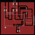
What I'm currently doing is putting a rectangular pad on the edge, turning off the stop and cream for the pad, then filling the rest with a polygon of copper. I can then attach a wire to the net in board layout.

But for the ground when I do a ground fill it only attaches to the pin inside the polygon not all of the polygon layout for the ground. And I need to connect all of it for good heat management.

How do you guys do LGA ICs.

Thank you all for your help.

project1.pngproject1.pngScreenshot_2015-12-13-16-49-02.pngproject2.png
 
Last edited:

You should always design a footprint in a generic way, this allows reuse of footprints.

So for a LGA define all the seperate pins. In the layout you can add the planes.
 

Hi,

Hint: although you have a lot of GND pins, you only need one pin at the symbol.

In the device configuration you need to connect multiple pads to one symbol pin.
So you will see a simple symbol.

When you define the polygons in board, then they are connected automatically, on the top layer.

Klaus
 

It is possible to make footprints with odd pad shapes, but even when you do it properly the DRC will give you overlap errors, which you must ignore.

But for your case I agree with senilicus, your device has an array of square pads, so your footprint should be similar. The polygons connecting groups of pins are better done in the layout view, not the footprint.
 

after.pngbefore.pngAll,

Thank you guys for your help! Very helpful community.

I reverted my footprint as per LGA layout of all pins, connected them all to their corresponding pins so only show 1 pin in symbol.

Is it okay to put a polygon plane over the common pins for one signal with no thermals? Will this make it impossible to solder?

One odd thing that happens is, when I define the name so that polygon is the same as the net, after placing the ground polygon it routes through
the signal polygons.

What am I doing wrong? Ha ha.
 

Hi,

Is it okay to put a polygon plane over the common pins for one signal with no thermals? Will this make it impossible to solder?
I don't expect problems without thermals, because the whole PCB including the devices is heated to the same temperature. You need a slow temperature rise rate to avoid moving of the device when the solder becomes liquid unequally. But best is to contact your assembling company on this.

In case EAGLE has problems with routing polygons inside a polygon, then try to
* either draw a small Gnd polygon,
* or draw lines in the top_restrict layer to isolate the polygons.

Klaus
 

We rarely use thermal relief on SMD assemblies, especially when SMPS's are involved or high power. As Klaus has said its all down to correct pre-heating, gently raising the whole assembly to the correct temperature, no thermal shocks....
If it is done correctly you will have no problems. Its like tomb stoning of chip components, if it happens you have BIG problems with your re-flow set up as you are creating quite a large temperature gradient across a small component. This use to happen with some early infra red ovens that had a wall of heat where the assembly entered the reflow zone! Not good. In 30 years I have only hear of a couple of tomb stoning problems.... Recently did a 4/6oz mixed board with no thermal relief on anything:)
 

Hi,

I don´t expect tomb stoning with that big IC.

But we had tomb stoning many years ago when we used wrong (too big) SMD pads for 0805 or 0603 chip rsisitors.

Read about pad recommendations (also temperature profile at soldering) at the manufacturer of the IC or read IPC recommedations.


Klaus
 

Thanks for all the information. I guess certain things will come with the more experience I get with designing PCBs. Of all the
forums that I'm a member of this is the most informative one out there, every time I ask a question you guys give answers.

What I needed to do was to change the rank of the GND polygon to a higher rank than all the other polygons.

solved.png

- - - Updated - - -

Dude! Thank you for the IPC reference, it's like NEC/IEC codebook for PCBs.
 

Status
Not open for further replies.

Part and Inventory Search

Welcome to EDABoard.com

Sponsor

Back
Top