Analysing the LVDS CMFB feedback circuits
- Thread starter asuprash
- Start date
- Status
- Not open for further replies.
ravet
Member level 5

AA
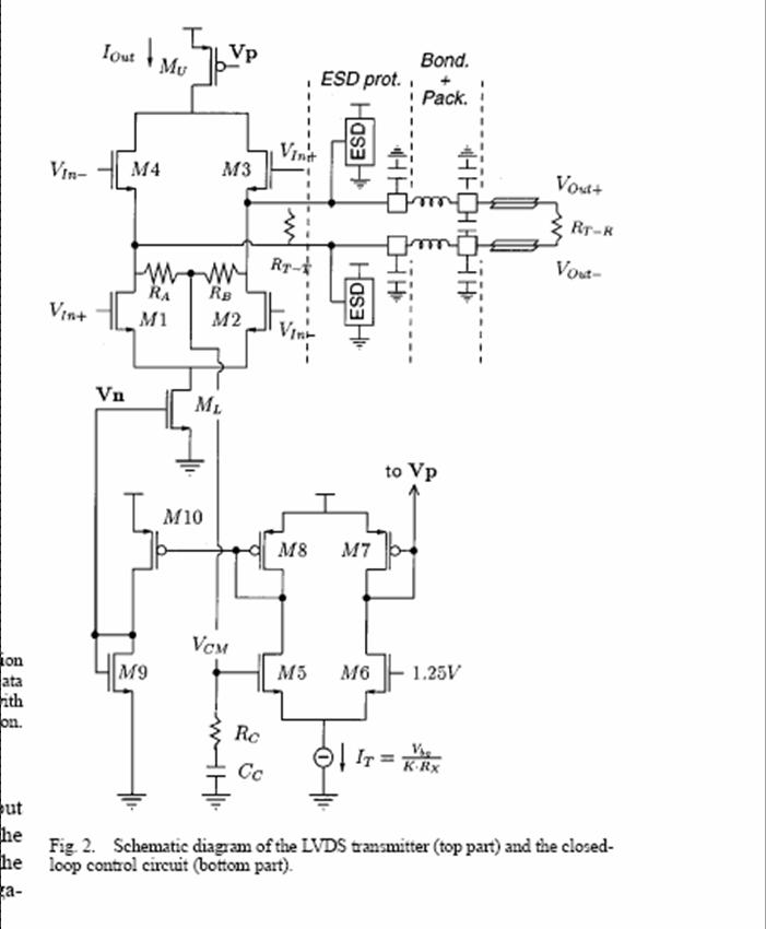
Vcm increases, current in the left leg decreases , leads to decrease in the Vp, as we should need smaller Veff to pass smaller current with same W/L ratio, when Vp decreases, current Iout increases, which in turn decreases Vcm, as seen, it is a -ve feedback, about the R-C network, it is to compensate for the CMFB stability , it is inserted in the loop , so that it can compensate for stability , you can use cap. only if this enough to stabilize the circuit, if not enough , you might use R and C, you should first check the CMFB stability before adding the R-C network, and see if it is worth adding them
Vcm increases, current in the left leg decreases , leads to decrease in the Vp, as we should need smaller Veff to pass smaller current with same W/L ratio, when Vp decreases, current Iout increases, which in turn decreases Vcm, as seen, it is a -ve feedback, about the R-C network, it is to compensate for the CMFB stability , it is inserted in the loop , so that it can compensate for stability , you can use cap. only if this enough to stabilize the circuit, if not enough , you might use R and C, you should first check the CMFB stability before adding the R-C network, and see if it is worth adding them
renwl
Advanced Member level 1
- Joined
- Apr 26, 2004
- Messages
- 452
- Helped
- 27
- Reputation
- 54
- Reaction score
- 5
- Trophy points
- 1,298
- Location
- shanghai,china
- Activity points
- 1,805
Vcm increase. the current in MU decrease, and the current in the ML increase. so the Vcm will decrease and the CMFB is functional.
asuprash
Newbie level 6
Rewat,
U r wrong there... I was thinking about this and the correct explanation is:-
Vcm increases-> current in left leg increases -> current in right leg decreases->
Vp increases -> I(Out-Top) decreases
Vn increases-> I(Out-Bottom) increases
Since, I(Top) and I(Bottom) are now unbalanced Vcm has to fall to limit the flow
of current in the bottom tail transistor.
What I fail to understand now is -> Why do we have to give feedback to
the bottom tail source ? Why not bias it at a constant value ?
ravet
Member level 5
ravet said:AA
Vcm increases, current in the left leg decreases , leads to decrease in the Vp, as we should need smaller Veff to pass smaller current with same W/L ratio, when Vp decreases, current Iout increases, which in turn decreases Vcm, as seen, it is a -ve feedback, about the R-C network, it is to compensate for the CMFB stability , it is inserted in the loop , so that it can compensate for stability , you can use cap. only if this enough to stabilize the circuit, if not enough , you might use R and C, you should first check the CMFB stability before adding the R-C network, and see if it is worth adding them
replace left leg with right leg, it is now true
engrvivs
Junior Member level 3
Hi Prashanth,
This is in response to ur query, "What I fail to understand now is -> Why do we have to give feedback to the bottom tail source ? Why not bias it at a constant value ? "
My contention is that in the present case, wherein both both Vn and Vp are trying to control the value of Vcm, the -ve feedback will be more quicker than in the case wherein we may fix the value of the lower bias, Vn.
In case u find the argument specious, plz correct me.
Regards,
Vivek.
Btrend
Advanced Member level 1
i agree with engrvivs's point.
there r 2 CMFB path, (1) is M5--> M7--> MU --> Vcm,
(2) is M5 --> M8 --> M10 --> M9 --> ML --> Vcm.
and path (1) should be slower than path (2), cuase MU has a high impedance load, while ML has a low impedance load.
using path (2) only is not a good idea, cause it maybe too slow to meet the spec.
there r 2 CMFB path, (1) is M5--> M7--> MU --> Vcm,
(2) is M5 --> M8 --> M10 --> M9 --> ML --> Vcm.
and path (1) should be slower than path (2), cuase MU has a high impedance load, while ML has a low impedance load.
using path (2) only is not a good idea, cause it maybe too slow to meet the spec.
- Status
- Not open for further replies.
Similar threads
-
Assistance with Switched-Capacitor Common-Mode Feedback (SC-CMFB) Circuit Issue
- Started by Serino
- Replies: 5
-
-
-
Help comparing two fully differential circuits with CMFB
- Started by PEEMONGER
- Replies: 2
-
Testing feedback functionality of an analog PID controller
- Started by yefj
- Replies: 1


