Continue to Site

Welcome to EDAboard.com

Welcome to our site! EDAboard.com is an international Electronics Discussion Forum focused on EDA software, circuits, schematics, books, theory, papers, asic, pld, 8051, DSP, Network, RF, Analog Design, PCB, Service Manuals... and a whole lot more! To participate you need to register. Registration is free. Click here to register now.

Analysing below circuit

Status
Not open for further replies.

circuitking

Full Member level 5
Full Member level 5
Joined
Jan 8, 2018
Messages
291
Helped
1
Reputation
2
Reaction score
1
Trophy points
18
Activity points
2,503
Hi all,
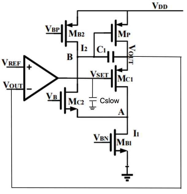
I would like to analyse the circuit.
how to draw the small signal model for the two loop circuit below.
How to calculate the pole frequencies from each loop
How to calculate the PSRR of the circuit
How do I determine the value of the C1 and Cslow so that the circuit is stable?
What should be the specifications of the opamp such as, gbw, gain.. etc

How to do the first cut design for the circuit.

Any help is appreciated thanks
1689171479318.png
 

I would not even try, as many of the elements have
significant C-V swings and you'd have to do a number of
closed-form calculations @ bias-points to "put a box
around it".

But that's from an "actually doing it" perspective, not a
"finish the assignment" one.

I don't like the Cslow idea, it will add phase lag which is
the opposite of what stability wants. Baggage on top of
any internal compensation in the op amp. If you really
want to compensate with shunt-C after the main amp then
maybe you want an uncompensated op amp. But then
Cslow will have to be electrically large (by IC standards)
or you may need to add a series R between amp output
and MC1 gate. But you def don't want to keep stacking
poles, rather than making one that's right.
 

Your Circuit is basically a Flipped Voltage Follower (FVF) Amplifier biased with an separate OpAmp.

You have 2 loops in operation,
  1. Vout -> A ->B ->Vout Loop which is the FVF Loop or the inner loop.
  2. Vout -> Opamp negative -> Vset which is the outer loop.
You would use this such that,
The inner FVF loop is lower gain but larger bandwidth and hence gives a better transient response.
The outer loop is a slower loop which provides large DC gain and ensures accuracy.

the Cslow basically is used to stabilize the outer loop (with the large rout of the opamp design). It also provides a filtered reference to the inner FVF loop. Here I am assuming that the opamp is uncompensated/output pole compensated.

C1 can be used as a miller cap to stabilize the inner FVF loop.

Search for "Cascoded Flipped Voltage Follower" for more.
 

It also provides a filtered reference to the inner FVF loop.
Thanks for the good explanation. You mean Cslow provides filtered reference to the inner FVF loop? is this the Vset?. filtering due to cslow and output resistance of opamp?

  • I am looking for the equations for gain and bandwidth of the inner loop and DC gain and bandwidth of the outer loop in terms of usual LDO specifications.
  • How do we decide the ratio between inner loop bandwidth and output loop bandwidth

I have searched for Cascoded Flipped Voltage Follower, found just one IEEE paper, I will go through that get back if I get answers to what I am looking for.
 
Last edited:

Thanks for the good explanation. You mean Cslow provides filtered reference to the inner FVF loop? is this the Vset?. filtering due to cslow and output resistance of opamp?
Yes

  • I am looking for the equations for gain and bandwidth of the inner loop and DC gain and bandwidth of the outer loop in terms of usual LDO specifications.
  • How do we decide the ratio between inner loop bandwidth and output loop bandwidth
You have a loop within a loop. And hence you have to analyse it as such. The bandwidth of the two loops and their individual stability will affect the other.
Usually you want the Faster Loop UGB to be much beyond the UGB of the Slower loop so that they don't interact.
I.e.m from the Slow loop perspective, the fast loop is like an ideal loop with infinite BW, and from the fast loop perspective, the slow loop is like a DC source.

I have searched for Cascoded Flipped Voltage Follower, found just one IEEE paper, I will go through that get back if I get answers to what I am looking for.
Try CAFVF and LSFVF, Bufferef FVF as keywords. There are quite a few results with those.
 

Status
Not open for further replies.

Similar threads

Part and Inventory Search

Welcome to EDABoard.com

Sponsor

Back
Top