Continue to Site

Welcome to EDAboard.com

Welcome to our site! EDAboard.com is an international Electronics Discussion Forum focused on EDA software, circuits, schematics, books, theory, papers, asic, pld, 8051, DSP, Network, RF, Analog Design, PCB, Service Manuals... and a whole lot more! To participate you need to register. Registration is free. Click here to register now.

[SOLVED] American/European way of drawing circuits?

Status
Not open for further replies.

dadili

Junior Member level 2
Joined
Oct 31, 2011
Messages
22
Helped
0
Reputation
0
Reaction score
0
Trophy points
1,281
Activity points
1,413
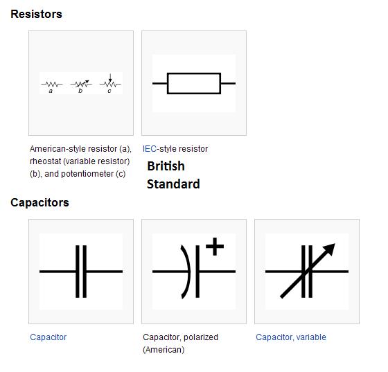
My professor told me that I have mixed circuit, little bit of european and little bit of american symbols, marking, labeling... what that supposed to mean?
this is my circuit **broken link removed**
 

Hi Gentleman!
I suspect , that his mean is the symbols of , your components , such as your capacitor , because , we have some symbols for capacitors .
Best Wishes
Goldsmith
 

Thank you. I really dont know what he meant and he wouldn't told me.
 

The Americans have their standard to draw each things ( and their standard is better) . ( that the IEEE authorized them)
For example they have the standard for names of components , such as diodes : 1N4148 or 1N4007 or etc .
but the europeans have their special standard . for example , refer to the symbol of nand gate in american books , it is different with the things that you can see at the europeans book!
Respect
Goldsmith
 
  • Like
Reactions: dadili

    dadili

    Points: 2
    Helpful Answer Positive Rating
thank you, I think I understand now
 

  • Like
Reactions: dadili

    dadili

    Points: 2
    Helpful Answer Positive Rating
One obvious example is that you used two different symbols for resistors. The zigzag line is of American origin while the rectangle is the European version. It doesn't matter which style you use as long as you stick to one style in the same diagram. Your professor was probably objecting to the mixing of two styles on the same schematic, and I agree wih him. It's not really a matter of right or wrong, but simply good practice to stick to the same style.

There's also the matter of crossed unconnected lines as that near pin 14 of the right-hand SN74LS90. If you use a blob (small filled circle) at connection points, it's not necessary to curve one line (usually a semi-circle) at unconnected crossings. In one older style, connected lines simply meet at a point without any blob, and unconnected crossings are depicted with the small semi-circle. But this style has largely fallen out of favour.

Another thing I'd like to point out is the blobs you've placed at line corners where nothing else connects to them, such as those below C1 and pin 5 of the 555. Those blobs are not needed.
 
  • Like
Reactions: dadili

    dadili

    Points: 2
    Helpful Answer Positive Rating


44_1326896247.jpg


Hope this helps.
Tahmid.
 
  • Like
Reactions: dadili

    dadili

    Points: 2
    Helpful Answer Positive Rating
thank you all for helping me. I've fixed everything now.
 

Status
Not open for further replies.

Part and Inventory Search

Welcome to EDABoard.com

Sponsor

Back
Top