dpaul
Advanced Member level 5

This is a question on the best practice involved for AMD 7Series FPGA for its configuration debuging.
Background:
An external Flash is connected to the 7 series FPGA and is supposed to configure it using the Master Serial Peripheral Interface (SPI) configuration mode x1 (board schematics exist, hardware bring up test not yet done). When the boards arrive, my objective is to test if the bitstream has been correctly loaded or not. Note that an option to program the FPGA over JTAG also exists (changing the values of M2, M1 and M0 pins ), but that is not my first target to test.
What info I have:
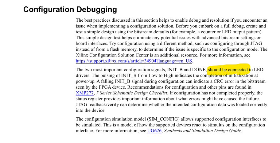
Now I referred to this document - 7 Series FPGAs Configuration User Guide, UG470 (v1.17) December 5, 2023
From page 15, I extract the following info...

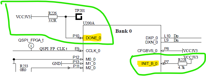
But what is mentioned in the above doc, I do not see in the schematic prepared by the PCB design engineer. This is what he has done...

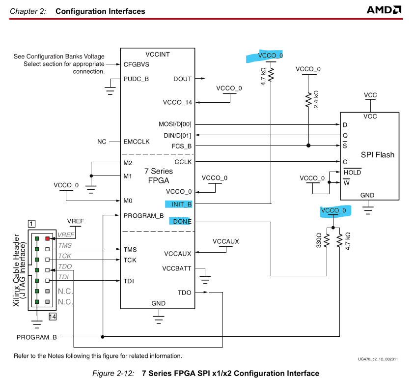
Well the above is also correct. In fact such an approach is mentioned within the same documentaion at page 48 (SS below).

Question:
So now I am confused as to what is the best approach for the INIT_B and DONE pins?
My main target will always be to how if bitstream loading from Flash to FPGA is successful or not.
Background:
An external Flash is connected to the 7 series FPGA and is supposed to configure it using the Master Serial Peripheral Interface (SPI) configuration mode x1 (board schematics exist, hardware bring up test not yet done). When the boards arrive, my objective is to test if the bitstream has been correctly loaded or not. Note that an option to program the FPGA over JTAG also exists (changing the values of M2, M1 and M0 pins ), but that is not my first target to test.
What info I have:
Now I referred to this document - 7 Series FPGAs Configuration User Guide, UG470 (v1.17) December 5, 2023
From page 15, I extract the following info...
But what is mentioned in the above doc, I do not see in the schematic prepared by the PCB design engineer. This is what he has done...
Well the above is also correct. In fact such an approach is mentioned within the same documentaion at page 48 (SS below).
Question:
So now I am confused as to what is the best approach for the INIT_B and DONE pins?
My main target will always be to how if bitstream loading from Flash to FPGA is successful or not.
