Continue to Site

Welcome to EDAboard.com

Welcome to our site! EDAboard.com is an international Electronics Discussion Forum focused on EDA software, circuits, schematics, books, theory, papers, asic, pld, 8051, DSP, Network, RF, Analog Design, PCB, Service Manuals... and a whole lot more! To participate you need to register. Registration is free. Click here to register now.

altium via stitching error

Status
Not open for further replies.

ultrasonic.1991

Member level 3
Member level 3
Joined
Nov 6, 2015
Messages
60
Helped
0
Reputation
0
Reaction score
0
Trophy points
6
Activity points
554
Hi, i'm desiging a pcb in Altium 17 and I want to use polygons for ground and VCC for better noise performance. But when i want to create via stitching an error appears that says
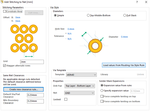
"unable to locate any suitable locations on net gnd"
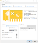
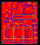
I attached screenshots of the setting that i used and also my pcb can anyone tell me what is the problem?
via stitching setting.png
polygon setting.png
pcb.png
 

You have connected top and bottom copper pours to different nodes (VCC and GND). There are no routes or copper pours on top side the could be connected to bottom copper by automatic via stitches. Connection of individual ground pins can be routed manually.
 
Status
Not open for further replies.

Part and Inventory Search

Welcome to EDABoard.com

Sponsor

Back
Top