Continue to Site

Welcome to EDAboard.com

Welcome to our site! EDAboard.com is an international Electronics Discussion Forum focused on EDA software, circuits, schematics, books, theory, papers, asic, pld, 8051, DSP, Network, RF, Analog Design, PCB, Service Manuals... and a whole lot more! To participate you need to register. Registration is free. Click here to register now.

Altium designer PCB - changing selection behavior?

Status
Not open for further replies.

rehakm

Junior Member level 1
Joined
May 31, 2011
Messages
15
Helped
1
Reputation
2
Reaction score
1
Trophy points
1,283
Activity points
1,421
Hi,
is it possible to change bahavior of selection that it will select object only in active layer? I found it anoying when I have components placed in top and bottom layer and when I want to select and move objects on top layer it displays selection dialog where I must confirm object that I want to select and then I can finally move it.
I can imagine that it would be better if object from active layer will be selected by default (single click then action) and if I want selection menu I would e.g. press CTRL and then click. Can I customize this?
I know I can press SHIFT+S to hide all but current layer and then it behaves as I want but I don't see other layer that I want to see.
 

Hi. I found it annoying too. For placement I always create "Layer sets": Top layer, Bottom layer, Top & Bottom layer. It's easy to switch between them and it's very useful. Other options are to lock the large components - they will not be "picked" or use filter to "Mask" objects on the layer what you would like to use.
 

Yes I made some layer presets but even if bottom is hidden and I click a component on top it will display selection menu including component from bottom. Also it would be usefull to exclude pads from selections. OrCAD do it different way, 1st you need to choose what object to manupulate (components or tracks or obstacles or...) and then simple click and modify them.
I'm also disappointed by edit routed traces. Esp. when I move a routed VIA the neighbour segments don't move together and it makes total mess. Also selection of track segments is often slowered by selection menus. Partial unrouting is problematic too, In OrCAD I just click one segment and pressed DEL one or more time and it deleted segment by segment until reaching the pad and I didn't need to click again again... I hope I will found as good way in Altium or does all other users only autorouters?
 

...Also it would be usefull to exclude pads from selections. OrCAD do it different way, 1st you need to choose what object to manupulate (components or tracks or obstacles or...) and then simple click and modify them.

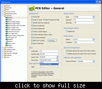
Try "Shift Click To Select" option in PCB Editor General Preferences - I personally select just tracks with a single click.

I'm also disappointed by edit routed traces. Esp. when I move a routed VIA the neighbour segments don't move together and it makes total mess. Also selection of track segments is often slowered by selection menus. Partial unrouting is problematic too, In OrCAD I just click one segment and pressed DEL one or more time and it deleted segment by segment until reaching the pad and I didn't need to click again again... I hope I will found as good way in Altium or does all other users only autorouters?

Yes, it's like that but you'll hopefully get to use.
 

>robertferanec

Yes I learned how to make own layer set. I also revealed the problem - why bottom objects was included in selection. It is because I had enabled mechanical layer 15 that I use for component outline (have drawn outlines for every component in my library). When I disable this layer in layer set then bottom components become really hidden. BUT, I like to see component outlines in top layer. It's problem because mechanical layer 15 is common for both components in top and bottom. I would need that if I flip a component from top to bottom it will switch outline layer to e.g. mechanical 14 or 16 so I would be able to recognize them. I mean same behavior like top overlay and bottom overlay. If it is possible to define 2 layers to be opposite each other...

>androm
shift+click will only help me to select more segments but when the segment is laying entire on pad it will bother with selection dialog again...

Anybody know how to set routed track to follow moved vias or components? OrCAD did it poorly but better than nothing...
 
Last edited:

I would need that if I flip a component from top to bottom it will switch outline layer to e.g. mechanical 14 or 16 so I would be able to recognize them. I mean same behavior like top overlay and bottom overlay. If it is possible to define 2 layers to be opposite each other...

Ah, loosemoose already answered this, I paste it here:

If you place components on top and bottom layer you will need to create a mechanical layer pair for the assembly layers. Hit"L" and then you will see on the bottom left corner "Layer pair".

This solved visibility of bottom objects but introduced a mess because I have already placed all components to both layers and now when defined mechanical layer pair the outlines are all in same layer and when I flip the component from bottom to top it changes outline layer opposite that I want, agrh...
 

Consider a complex footprint is created (on top side of PCB) using some layer set including some mech layers. If you gonna flip that comp to the bottom side and would like to see all the mech layers separately you should properly pair them in PCB Editor every time while creating a new PCB file - that's one of the first things to do before comps placement. BTW have you tried IPC Footprint Wizard yet in library editor? You can get an idea of layer usage from there: Mech15 is supposed to provide courtyard area and Mech13 is for body graphics. So in this case if such a footprint should be placed on opposite PCB side those layers should be paired with lets say Mech14 and Mech16 respectively. Once done every footprint would display mech layers accordingly and you'd be able to manipulate them during assembly outputs creation. A little piece of advice here: don't mix body graphics and 3d body projection on the same layer like the IPC Wizard does that on Mech13 - there is a plenty of free layers left for your disposal so place step models somewhere else.
 
  • Like
Reactions: rehakm

    rehakm

    Points: 2
    Helpful Answer Positive Rating
>androm
Yes you're right. I didn't defined layer pairs before placing and make this trouble myself. But fortunatelly there are not too much components so I was able to go to PCB list and change tracks of bottom placed components to opposite layer and then defined the proper layer pair. I also make a template with some basic definitions so I should avoid this in future. Now the selection with enabled top/bottom layer set is easier because hidden componens are not selectable. Solved.

But how about moving routed vias and components? Any suggestion how to move end segments together?
 
Last edited:

To shift tracks connected to via first select the via then click on it and drag.
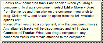
If you want to relocate a routed component set Comp Drag to "Connected Tracks" in PCB Editor General Options and use the procedure provided with context help: select Edit>Move>Drag.
I have no idea how that fits you but it's working anyway.

99_1308232370.gif
 
  • Like
Reactions: rehakm

    rehakm

    Points: 2
    Helpful Answer Positive Rating
>androm
Thanks, I had Comp Drag to "none" in default settings. I also didn't know, theres different move than dragging by mouse. Well now I can move routed vias and traces are moving together, respecting angles and DRC. But when I do it on a component it moves traces by any angle and don't respect DRC, traces are overlaying each other and it takes quite a lot time to fix it...
 

Sorry for that indeed! There is only few ways I know and obviously you do: select Inside Area OR select comp and comp connections (Edit>Select>Component Connections) then move all the things by Move Selections command. Good luck!
 

Status
Not open for further replies.

Part and Inventory Search

Welcome to EDABoard.com

Sponsor

Back
Top