Lucast85
Member level 3

Hi all,
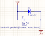
I'm designing the schematic of a project and I want to constraint the person who design the layout of board to place some components on bottom layer of PCB.
As suggested in this thread (https://www.edaboard.com/threads/349428/), I add as a parameter of the component the rule that indicate to place the component on bottom side. It seems all ok, but during layout design I cannot see the violation of that rule.
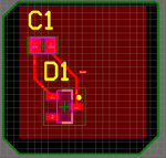
The component is now on the top layer but no error was reported.
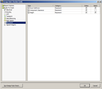
In the design rule checker, under the menu placement, there are only:
Why there is the rule, but there is no-way to see the violation of that rule?
THanks !
I'm designing the schematic of a project and I want to constraint the person who design the layout of board to place some components on bottom layer of PCB.
As suggested in this thread (https://www.edaboard.com/threads/349428/), I add as a parameter of the component the rule that indicate to place the component on bottom side. It seems all ok, but during layout design I cannot see the violation of that rule.
The component is now on the top layer but no error was reported.
In the design rule checker, under the menu placement, there are only:
- Room Definition
- Component Clearance
- Height
Why there is the rule, but there is no-way to see the violation of that rule?
THanks !


