Continue to Site

Welcome to EDAboard.com

Welcome to our site! EDAboard.com is an international Electronics Discussion Forum focused on EDA software, circuits, schematics, books, theory, papers, asic, pld, 8051, DSP, Network, RF, Analog Design, PCB, Service Manuals... and a whole lot more! To participate you need to register. Registration is free. Click here to register now.

[ADS] Voltage Multiplier and its input impedance in ADS ??

Status
Not open for further replies.

kela3kela

Full Member level 4
Full Member level 4
Joined
Apr 30, 2009
Messages
191
Helped
5
Reputation
10
Reaction score
5
Trophy points
1,298
Activity points
2,502
Respected Members,

I have designed a voltage multiplier/Doubler at 950 MHz (0.95 GHz)(Figure below). I am having some trouble in terms of its functionality and design. If you could clarify the following;

1. Is my circuit design appropriate/correct (i.e. simulators, lumped components, values, and rest parameters)?
2. Why Im not getting any input voltage Vcc and its multiplied output voltage Vout?
3. Any help available or a sample design tutorial in ADS for a voltage multiplier?
4. Finally, I would like to find out what is the input impedance of the circuit at different input power and frequency so that I can proceed with the design of an impedance matching network which will be placed in between a 50 ohm antenna and the voltage doubler. May I know how can I do that in ADS?

VD 950 MHz.jpg
Output.jpg
Could anyone please help?
Thanks.
 

From first look, your source works with 0.95 Hz! not GHz. As I understood, you want to rectify your voltage and have some DC-voltage? You can easily plot impedances vs. frequency with for example s-paramters. Just have a look in the manual.
 
Last edited:

1 and 2) are you sure about the 0.95 GHz working frequency and 3.3 Farad capacitors?
Note that your Source is working at 0.95 Hz while your HB simulation is running at 0.95 GHz

3) There is no ADS Design Guide for Voltage Doublers (that I know of)

4) If you want to know the input impedance perform Large Signal S-Parameter Simulation (LSSP) and plot the reflection coefficient (S11) of the circuit in a Smith Chart

Best regards and good luck
 

@johnjoe: @viper_iv

sorry about the values mistake..My source is 0.95 GHz and C=3.3 nF with R=100 Kohm...Figure updated...And yes I need to rectifiy my circuit to get a DC voltage..
So any helot abt Voltage doubler frm this updated figure given below...

Updated.jpg
 

The configuration you have is working for me (I get a 1.08 V signal at the output)

However, you should only use the Harmonic Balance and Large-Signal S parameters solvers for this case (not AC)
 

Im still not getting any input or output voltage..
@viper_iv: Could u kindly share ur ADS file that produced the results at ur end.
 

Here you go...
 

Attachments

  • multi.zip
    14 KB · Views: 177
Is the file provided an ADS file..Its not supported..
 
Last edited:

@johnjoe: I re-did the simulation and I'm getting output and input wave forms but the output is not Doubled...Images attached...Any reason u knw of?? Anyone ...
Circuit.jpg
Results ADS.jpg
 

First, it's ads 2011 schematic file, you have to import the file into the library directory of an existing project. For first try, remove the coils and the 1pF cap. I used the ideal diodes with your model specification, maybe try this.

I added my sim and schematic pics and the complete ads 2011 project.
 

Attachments

  • 1.jpg
    1.jpg
    448.1 KB · Views: 274
  • 2.jpg
    2.jpg
    469.5 KB · Views: 266
  • multi.rar
    24.3 KB · Views: 139
Last edited:
  • Like
Reactions: kela3kela

    kela3kela

    Points: 2
    Helpful Answer Positive Rating
    V

    Points: 2
    Helpful Answer Positive Rating
Thankyou for the project, Ill continue with the structure first without coils and thn making the doubler.Thnx again
 

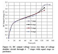
@johnjoe: One more query. I want to know how many stages would produce the max DC voltage. I have seen a paper where its plotted as below.
Is there any function in ADS to use a single voltage doubler , make its [n] stages and see the DC results??


@johnjoe:
I added additional 7-stages of Voltage doubler to your design in-order to get more output DC Voltage but its not improving. Should I attach the file?
 

@johnjoe:
I added additional 7-stages of Voltage doubler to your design in-order to get more output DC Voltage but its not improving. Should I attach the file?

You can upload if you want.
 

Please post everything in the forum, not as private message.
First mistake: Your source frequency is 0.95 GHz, your HB-frequency is 0.95 Hz, change the value of swp_freq.
Second mistake: The circuit is not correct ;-). I uploaded a corrected version. Steady state solution shows an multiplied voltage but from transient analysis it's obvious that it takes some time, maybe you can optimize it.
 

Attachments

  • %Multi%Doubler.rar
    19.5 KB · Views: 143

Ok.I'll post everything here.
Thankyou for pointing out a major mistake. I'll update the circuit and report back soon.

- - - Updated - - -

@johnjoe: So As seen in the figures below, I get 1V at one stage multiplier. But when I move to two stage voltage doubler the voltage reduces to 14 mV with optimized C values.
File attached. Kindly assist.


Attachments

  • %Multi%Doubler.rar
    21.1 KB · Views: 126

Did you checked my uploaded schematic? It is a multi-stage voltage multiplier based on your Greichnacher circuit.
 

@johnjoe: Which uploaded file?? Can u kindly re-post the multistage file.

- - - Updated - - -

@viper_iv: Thnx for the link, but atleast I should get near to 5V for three stages...As pr theory
 

Status
Not open for further replies.

Part and Inventory Search

Welcome to EDABoard.com

Sponsor

Back
Top