Continue to Site

Welcome to EDAboard.com

Welcome to our site! EDAboard.com is an international Electronics Discussion Forum focused on EDA software, circuits, schematics, books, theory, papers, asic, pld, 8051, DSP, Network, RF, Analog Design, PCB, Service Manuals... and a whole lot more! To participate you need to register. Registration is free. Click here to register now.

ADS Substrate definition problem for polyimide flex

eieiguy

Newbie
Newbie level 1
Joined
Mar 28, 2024
Messages
1
Helped
0
Reputation
0
Reaction score
0
Trophy points
1
Activity points
24
My feeling is that I am overlooking something very simple. I've the defined the layers for a polyimide flex by modifying the TwoLayerFR4 template. I know that there is no longer a ground plane as I am routing an inductive coil antenna on both sides. Via Designer fails since there is no plane as a return path. My question is, what is the best way to specify a plane? Do I add a a second conductor to one side of the flex, and how would I specify it as a plane?
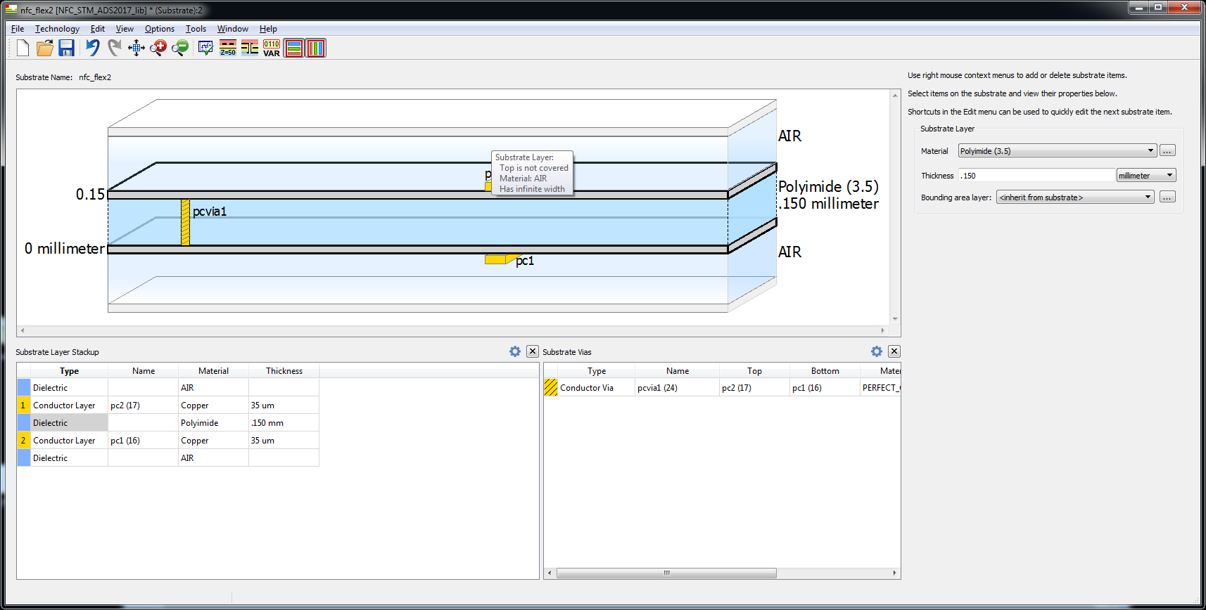
image_2024-03-28_123138707.png
 
You should define a padstack first then you have to define a via definition.
1711662208836.png

1711662171694.png

After all, you can place your via on the layout.This via can also be used for gnd! connection or interlayer connection while it's placed.
1711662033525.png
 
Last edited:

LaTeX Commands Quick-Menu:

Part and Inventory Search

Welcome to EDABoard.com

Sponsor

Back
Top