Continue to Site

Welcome to EDAboard.com

Welcome to our site! EDAboard.com is an international Electronics Discussion Forum focused on EDA software, circuits, schematics, books, theory, papers, asic, pld, 8051, DSP, Network, RF, Analog Design, PCB, Service Manuals... and a whole lot more! To participate you need to register. Registration is free. Click here to register now.

[SOLVED] ADS set gnd layer failed(the layer isnt a EM planar conductive layer)

Status
Not open for further replies.

timer000

Newbie level 4
Newbie level 4
Joined
Feb 13, 2023
Messages
6
Helped
0
Reputation
0
Reaction score
0
Trophy points
1
Activity points
102
Dear ALL, I encouted a problem about seting the feed points in ADS 2019.


I know while I set a postive port on layer1 , I also need to set a negative port.


Then, I know we might use a new function of ADS2019 to set a ground layer to instead seting negative ports one by one.


This is my subtract setting:
after importing the relative gerber files, I set L01_Top& L02_gnd as conductive layers.
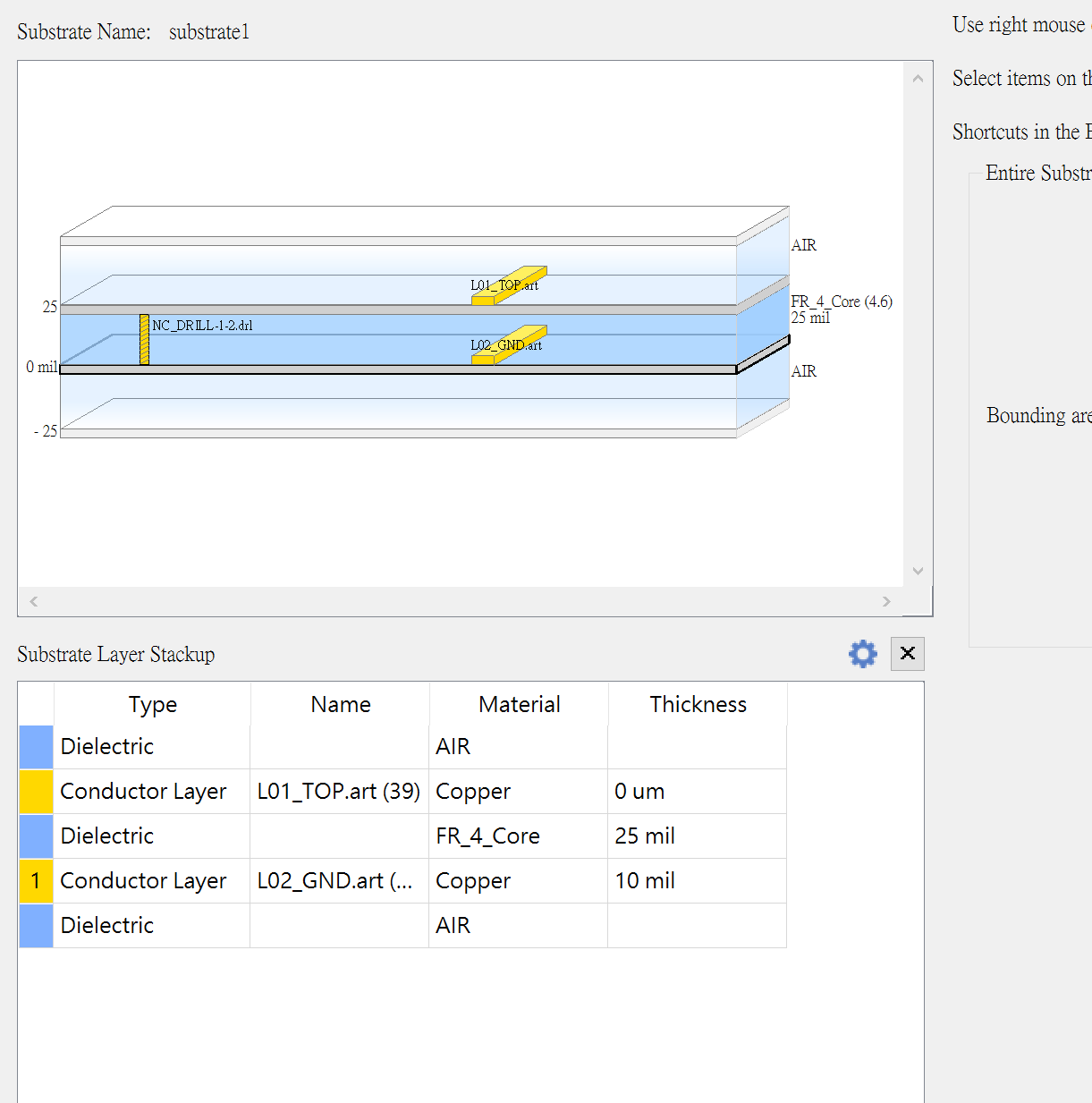
擷取.PNG


Afterward, I set “L02_Gnd” as the ground layer for P1&P2
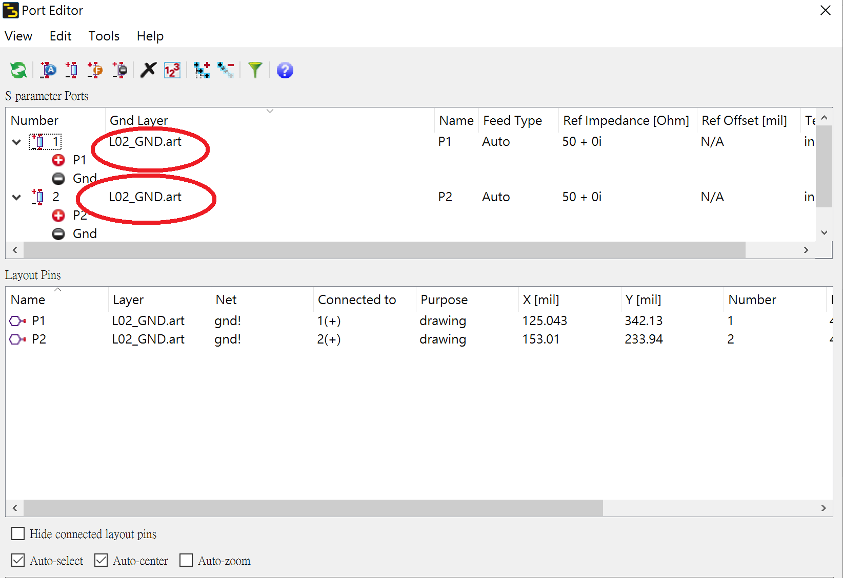

擷取2-1.png


Then, I want to run a simulation, then I see the following wrong message.
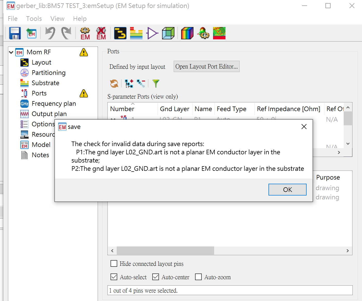
擷取3.PNG


But I think I already set L02_GND.art as a conductive layer.
After trying a lot of ways, I still cannot solve the issue.

May anyone help me?

Thanks
 

Overall your settings look ok, if your emSetup points to the substrate that you showed.

I only see one mistake: thickness for L01_TOP.art is defined as 0, but this doesn't explain your error message.
 

After seeing your advice, I tried a lot today.


Yesterday I set the port at the L02_Gnd.art.
That is a wrong setting, so I reset the port to L01_Top.
Just as the following picture:

擷取.PNG


However, the same wrong message still occurs.

On the other hand, if I don't use the ""ground layer" function in the windows of the port editor.
Instead, set 2 additional ports(port 3 & 4 ) on L02_gnd, then drag port3&4 to be the ground of port1&2.
The simulation can work.

But if I switch to my old way( set “L02_Gnd” as the ground layer for P1&P2), the wrong message is still the same as before.
I upload my ADS layout file to google driver:

https://drive.google.com/file/d/1FymM5JyD4Gnw8vNuMJmLA3SkxXveHxqn/view?usp=share_link

May someone help me?
I know I already received great help from you.
Thanks!
 
Last edited:

However, the same wrong message still occurs.

What ADS version did you use?
I tried your workspace and it simulates with no error messages on ADS 2022 Update 2.
Edit: I also tried your workspace ADS 2020, that worked as well.

In 3D EM preview, the port reference is shown on bottom layer as expected.

There is one mistake (unrelated to your error message) that I noticed when looking at 3D EM preview: thickness is 12µm for top layer and substrate, but 12 mils for bottom layer. It seems that you messed up units.
 
Last edited:

    timer000

    Points: 2
    Helpful Answer Positive Rating
This information is very important to me.
I use ADS 2019!

I am bothered by the issues these weeks.
I looked at so many tutorial videos, but still cannot find an answer.
Thanks for your kind information


Therefore, It might be a bug of ADS?
 

I agree, if the exact same workspace works in ADS 2020 but fails in ADS 2019 then it might be a bug in the old version. I don't have ADS2019 to test that.
 
Status
Not open for further replies.

Part and Inventory Search

Welcome to EDABoard.com

Sponsor

Back
Top