Continue to Site

Welcome to EDAboard.com

Welcome to our site! EDAboard.com is an international Electronics Discussion Forum focused on EDA software, circuits, schematics, books, theory, papers, asic, pld, 8051, DSP, Network, RF, Analog Design, PCB, Service Manuals... and a whole lot more! To participate you need to register. Registration is free. Click here to register now.

ADS Layout

errikosgk

Newbie level 6
Newbie level 6
Joined
Apr 12, 2024
Messages
12
Helped
0
Reputation
0
Reaction score
0
Trophy points
1
Activity points
103
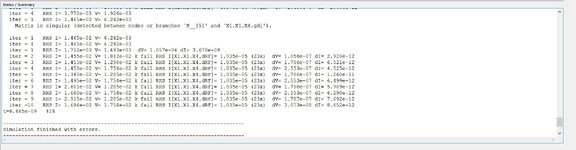
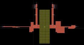
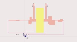
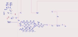
Hello, I am trying to do an em cosimulation in ADS but when I run the simulation it says that it is finished with errors like in the screenshot below. It says that matrix is singular beween nodes or branches.... but I cannot find these nodes in my layout. Can you help me?
 

Attachments

  • 5.jpg
    5.jpg
    211.4 KB · Views: 29
These errors are coming from an active model.
There might have few causes. Either model itself has some problems OR when it's been used with EM simulated board/substrate some convergence errors occur.
OR both..

Nobody can say something without knowledge of simulation setup.
I recommend you to check the board simulation results first, you shouldn't see any weirdness.
I checked the model and I can't find something weird
 
For every capacitor try putting a low-ohm resistor in series with it.

Some simulators require that every circuit have a ground icon somewhere.

Any PNP or Pmos should not receive bias voltage greater than its emitter leg.

Two supply rails (source or ground) must not be connected to each other unless a component is in wire between them.
This is the layout I am trying to cosimulate. Between the pads I have designed capacitors will be placed.
 

Attachments

  • 8.jpg
    8.jpg
    78.1 KB · Views: 25
  • 9.jpg
    9.jpg
    25.1 KB · Views: 26
  • 10.jpg
    10.jpg
    67.1 KB · Views: 24
Sorry but this layout is a nightmare.
You have to work on it and Momentum cannot simulate correctly this layout because it has many fundamental errors.( Ports, Transmission Lines) etc.
 

LaTeX Commands Quick-Menu:

Similar threads

Part and Inventory Search

Welcome to EDABoard.com

Sponsor

Back
Top