xzsawq21
Junior Member level 1

Hello
I have drawn a 6-layers layout in ADS.
I should have a ground plane and many ground vias on the top layer.
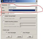
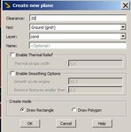
I have inserted a ground plane with 20mils clearance as shown below:


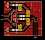
some area should be ground free as you see with Red Cross in above pic. how should I draw a keep-out layer?
some area I need to have many ground vias as you see with some Blue circles. is there any prepared multi-layer via?
the left pad of C3 capacitor is connected to ground as you see in above schematic, but why the ground plane is not unified with this pad?!!!
Thanks
I have drawn a 6-layers layout in ADS.
I should have a ground plane and many ground vias on the top layer.
I have inserted a ground plane with 20mils clearance as shown below:


some area should be ground free as you see with Red Cross in above pic. how should I draw a keep-out layer?
some area I need to have many ground vias as you see with some Blue circles. is there any prepared multi-layer via?
the left pad of C3 capacitor is connected to ground as you see in above schematic, but why the ground plane is not unified with this pad?!!!
Thanks

