Continue to Site

Welcome to EDAboard.com

Welcome to our site! EDAboard.com is an international Electronics Discussion Forum focused on EDA software, circuits, schematics, books, theory, papers, asic, pld, 8051, DSP, Network, RF, Analog Design, PCB, Service Manuals... and a whole lot more! To participate you need to register. Registration is free. Click here to register now.

Additive latency for DRAM READ and WRITE commands

Status
Not open for further replies.

promach

Advanced Member level 4
Joined
Feb 22, 2016
Messages
1,202
Helped
2
Reputation
4
Reaction score
5
Trophy points
1,318
Activity points
11,643
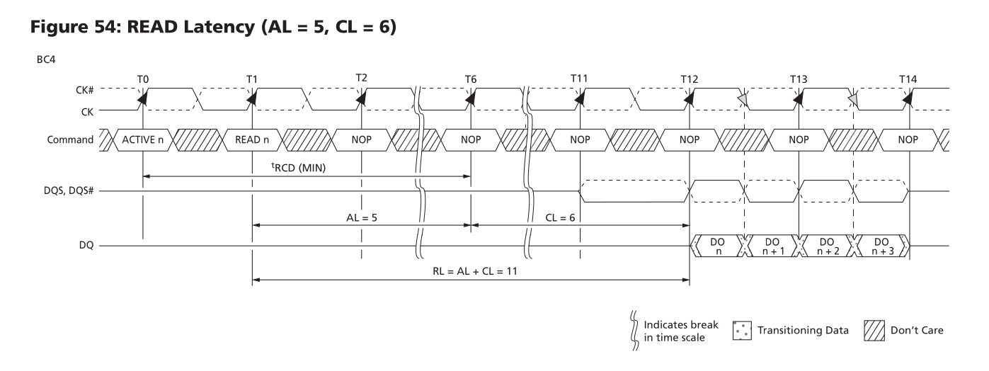
In TN-47-10 – DDR2 Posted CAS# Additive Latency Technical Note , what does it exactly mean by Additive latency (AL = 1) is only used for READ commands and will not affect WRITE command timing ?
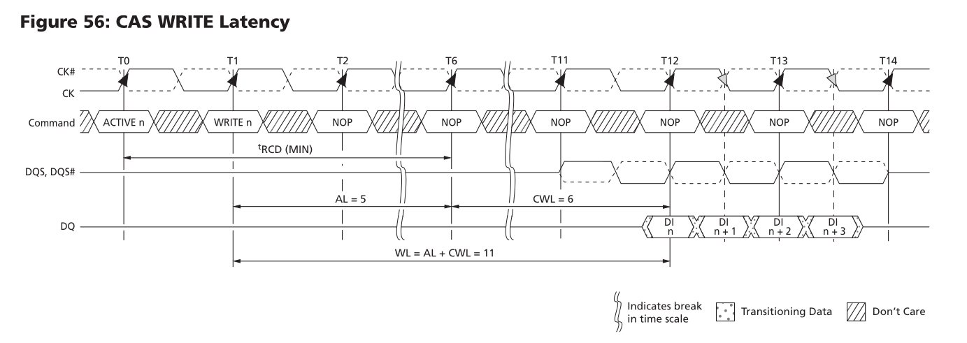
DRAM_write_latency.png


DRAM_read_latency.png
 

AL=1 seems to be handled specially. However, the same information can't be found in newer Micron DDR2 datasheets, thus I wonder if it applies to all devices.
--- Updated ---

TN-47-10 isn't available at micron.com, but several other TN-47-xx notes are. Suggests that it has been withdrawn.
 
Last edited:

Status
Not open for further replies.

Part and Inventory Search

Welcome to EDABoard.com

Sponsor

Back
Top