Maitry07
Full Member level 2

Hello,
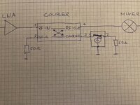
I have designed one RF front end for my 4 channel receiver which include COTS components from recognized manufacturers such as Bias tee, LNA, attenuator, 4 way power splitter and band pass filters for 4 bands.
I have taken proper care for impedance matching in the layout. But still, I wanted to put test/debug points in between the components so that I can also check individual component's performance with spectrum analyzer. so, what is the best method in RF to put test/debug points so that this insertion cannot add any impedance mismatch and parasitic capacitance. what is the best practice to put this kind of test/debug points in the RF pcb through which any components can be accessed and tested via spectrum analyzer and it cannot affect the main signal path or performance of the overall RF front end chain?
request you to provide solutions for the same


")