Continue to Site

Welcome to EDAboard.com

Welcome to our site! EDAboard.com is an international Electronics Discussion Forum focused on EDA software, circuits, schematics, books, theory, papers, asic, pld, 8051, DSP, Network, RF, Analog Design, PCB, Service Manuals... and a whole lot more! To participate you need to register. Registration is free. Click here to register now.

ADC noise caused by voltage regulators

Status
Not open for further replies.

serhannn

Member level 4
Member level 4
Joined
Sep 28, 2010
Messages
69
Helped
2
Reputation
4
Reaction score
2
Trophy points
1,288
Visit site
Activity points
1,939
Hi,

I have a design consisting of an analog part and a microcontroller board (LPCxpresso 1769 by NXP) with an integrated 12 bit ADC. For the operation of the circuit, I need ±5 V (for op-amps) and 3.3 V (to supply the microcontroller). When I supply the circuit with these voltages using a power-supply, I manage to get reasonably noise-free data from the output of the ADC. However, when I use two 9 V batteries and voltage regulators to obtain ±5V and 3.3V, significant amount of noise is added up to the output of the ADC. The linear voltage regulators I use are regular 7805, 7905 (negative voltage regulator) and an adjustable voltage regulator, LM317. I'm using 7805 for 5V, 7905 for -5V and LM317 for 3.3V. I'm using two 9V batteries, since I specifically use one of them (with reverse polarity) just for obtaining -5V and from the other 9V battery, I obtain +5V and 3.3V.

I would like to operate the circuit with batteries (both for portability and I thought that this would even reduce the noise further, eliminating the noise originated from the power-supply), but the results are not really encouraging. By the way, the circuit operates at very low frequencies (typically less than 10 Hz, near-DC values), therefore a high-frequency artifact is out of question, I think. Also, I checked out the datasheets of the regulators and connected appropriate capacitors between their ports (I used cap. values suggested in typical application circuits). When I look at the output of the regulators on the scope, I see very clear voltage signals, not swinging any more than 1-2 mV, so the signals seem to be quite stable, even more stable than those that had come from the power-supply before. However, when I receive data, there is a lot of noise added in the ADC output.

I do not really understand the source of the problem, what might be the cause of that noise? Why would voltage regulators add noise to the ADC output when their outputs, namely all input voltage signals are very stable? Also, if this is typical, is there any technique/additional circuit that should be used with voltage regulators to reduce or eliminate that noise? In the internet, I have encountered some suggested clear-up circuits, but I don't know if they are related or if they would work in this case, anyone has any suggestions regarding this?

Thanks a lot for your help.

Serhan
 

How does it look like and / or how is the frequency distribution (FFT option on oscilloscope, or from your data buffer in software FFT). Does it change when the processor is doing certain tasks? depending on the sample rate, type of converter and input filtering, there could be an aliasing problem due to out of band signals.
 

Two points:
- please specify significant amount of noise in terms of bits
- is the ADC reference stabilized or simply derived from a supply voltage?
 

The Good, The Bad, and The Ugly. Is No Noise Good Noise?
http://www.analog.com/library/analogDialogue/archives/40-02/adc_noise.html

Techniques that Reduce System Noise in ADC Circuits
http://ww1.microchip.com/downloads/en/DeviceDoc/adn007.pdf


ADC Noise Canceler

The ADC features a noise canceler that enables conversion during sleep mode to reduce noise
induced from the CPU core and other I/O peripherals. The noise canceler can be used with ADC
Noise Reduction and Idle mode. To make use of this feature, the following procedure should be
used:
1. Make sure that the ADC is enabled and is not busy converting. Single Conversion
mode must be selected and the ADC conversion complete interrupt must be
enabled.
2. Enter ADC Noise Reduction mode (or Idle mode). The ADC will start a conversion
once the CPU has been halted.
3. If no other interrupts occur before the ADC conversion completes, the ADC interrupt
will wake up the CPU and execute the ADC Conversion Complete interrupt routine. If
another interrupt wakes up the CPU before the ADC conversion is complete, that
interrupt will be executed, and an ADC Conversion Complete interrupt request will be
generated when the ADC conversion completes. The CPU will remain in active mode
until a new sleep command is executed.
Note that the ADC will not be automatically turned off when entering other sleep modes than Idle
mode and ADC Noise Reduction mode. The user is advised to write zero to ADEN before entering
such sleep modes to avoid excessive power consumption.

Page 207 in this doc :
http://www.atmel.com/Images/doc2570.pdf
 
An additional remark related to a common misunderstanding.
By the way, the circuit operates at very low frequencies (typically less than 10 Hz, near-DC values), therefore a high-frequency artifact is out of question, I think.
Your input signal is apparently low frequency, the data conversion rate is possibly low as well. The ADC however is rather fast, sampling the input voltage with a short aperture. This aperture window determines the bandwidth of the ADC measurement, regarding noise and the susceptibility to high frequency interferences. You'll need to filter ADC input voltage and reference effectively to get rid of high frequency interferences.

As an additional remark, by tying the ADC reference input directly to the 3.3V supply, the lpcxpresso designers clarified, that they didn't intend to make a high performance analog board.
 
How does it look like and / or how is the frequency distribution (FFT option on oscilloscope, or from your data buffer in software FFT). Does it change when the processor is doing certain tasks? depending on the sample rate, type of converter and input filtering, there could be an aliasing problem due to out of band signals.

The frequency distribution is gathered around DC. Before the ADC input, I'm filtering the received signal with an second-order low-pass filter with a cut-off frequency of 5.5 Hz, then I'm amplifiying it with a non-inverting op-amp with a gain of 4. I don't think the noise changes when processor is doing other tasks. It seems to be caused by the addition of the voltage regulators to the sytem.


Two points:
- please specify significant amount of noise in terms of bits
- is the ADC reference stabilized or simply derived from a supply voltage?

- Normally, when I supply the circuit from the power-supply the swing of a DC input is 1-2 points (using 12-bit ADC, there is a range of 4096 points). With regulated power, noise is around 20-30 points and there are a lot of glitches. I change nothing but supply the power from regulators (also, there are a number of capacitors for regulators).
- ADC reference input is tied to 3.3V.

The Good, The Bad, and The Ugly. Is No Noise Good Noise?
http://www.analog.com/library/analogDialogue/archives/40-02/adc_noise.html

Techniques that Reduce System Noise in ADC Circuits
http://ww1.microchip.com/downloads/en/DeviceDoc/adn007.pdf


ADC Noise Canceler

The ADC features a noise canceler that enables conversion during sleep mode to reduce noise
induced from the CPU core and other I/O peripherals. The noise canceler can be used with ADC
Noise Reduction and Idle mode. To make use of this feature, the following procedure should be
used:
1. Make sure that the ADC is enabled and is not busy converting. Single Conversion
mode must be selected and the ADC conversion complete interrupt must be
enabled.
2. Enter ADC Noise Reduction mode (or Idle mode). The ADC will start a conversion
once the CPU has been halted.
3. If no other interrupts occur before the ADC conversion completes, the ADC interrupt
will wake up the CPU and execute the ADC Conversion Complete interrupt routine. If
another interrupt wakes up the CPU before the ADC conversion is complete, that
interrupt will be executed, and an ADC Conversion Complete interrupt request will be
generated when the ADC conversion completes. The CPU will remain in active mode
until a new sleep command is executed.
Note that the ADC will not be automatically turned off when entering other sleep modes than Idle
mode and ADC Noise Reduction mode. The user is advised to write zero to ADEN before entering
such sleep modes to avoid excessive power consumption.

Page 207 in this doc :
http://www.atmel.com/Images/doc2570.pdf

Thanks a lot. Especially, the Microchip article has been very beneficial for my understanding. Also, I will take a lot at the "ADC noise canceler" and see if it will work in this case. It seems like a good idea to do the conversion in Sleep mode so that the noise from other peripherals can be reduced.

An additional remark related to a common misunderstanding.

Your input signal is apparently low frequency, the data conversion rate is possibly low as well. The ADC however is rather fast, sampling the input voltage with a short aperture. This aperture window determines the bandwidth of the ADC measurement, regarding noise and the susceptibility to high frequency interferences. You'll need to filter ADC input voltage and reference effectively to get rid of high frequency interferences.

As an additional remark, by tying the ADC reference input directly to the 3.3V supply, the lpcxpresso designers clarified, that they didn't intend to make a high performance analog board.

As I mentioned, there is low-pass filter before the ADC, but after low-pass filtering, I amplify the signals again (x4). Is it necessary to put another anti-aliasing filtering right in front of the ADC, meaning after the amplification stage. I thought that I'm already getting rid of the high-frequency artifacts before amplifiying the signal, so it is not really necessary to do another around of LP filtering.

Why do you think that tying the ADC reference directly to 3.3 V prevents the board from being a high performance? Should there be some sort of stabilization of the ADC reference as you mentioned in your previous post? I did not really catch the logic behind that.

Also, is there any kind of internal noise of voltage regulators that require any special treatment? I added some capacitors, as suggested in typical app circuits in their datasheets, but I'm wondering if there is anything more to be done.
 

Achieving 12 bit ADC accuracy on a general purpose microprocessor is demanding in any case. It will be rarely achieved with Vref conncted to Vdd. At least an effective filtering (e.g. ferrite bead or series resistor and 5 or 10 uF ceramic C) would be suggested. For absolute DC performance, you would want to connect a stable reference source.

I'm not sure what the main problem in your battery powered setup. Either it's a noise 3.3V supply or it's the way the analog input signal is interfaced to the board. You should be basically able to achieve the same ADC performance as in the previous test. May be a photo of the setup can clarify things.
 

I'm not sure what the main problem in your battery powered setup. Either it's a noise 3.3V supply or it's the way the analog input signal is interfaced to the board. You should be basically able to achieve the same ADC performance as in the previous test. May be a photo of the setup can clarify things.


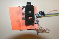
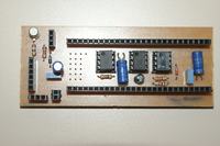
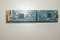
I uploaded some pictures of the setup above. I'm getting the optical signal from a sensor board, the signal is pre-amplified there and goes to the PCB, there it's buffered (leftmost opamp), low-pass filtered (middle) and amplified once more (right) As you see, there are some pins on the PCB, some of which I use for powering the op-amps and the microcontroller. The problem I mentioned occurs when I supply the power from 9V batteries with voltage regulators.
 

Is there difference between common ground paths when switching from battery power to mains derived power?

I mean changing the position of the ground that goes to the power supply (either battery of mains derived) may result in a piece of ground trace that contains both analog signal return and digital return. Same is valid for the positive supply, a common trace for both analog supply and digital supply may introduce noise.

Are you able to measure the analog input signal directly at the input of the ADC (both signal lead and ground lead as close as possible to the ADC inputs)? You may also measure directly the output of your preamplifier to figure out whether the noise is already present at the output of the preamp. If the signals are clear, then you may blame the ADC's reference voltage.

When measuring small signals close to digital ones, it is best to avoid the use of the probe's ground lead. Better is to connect the coaxial ground of the probe's input directly to the ground of the ADC. Several probes have some additional hardware that you can position over the probe tip to enable a ground connection via very short lead.

Wires between your amplifier and the ADC may pick up noise directly, or via common ground path. I don't know the features of the ADC, but adding a simple RC network directly at the input of the ADC may help. Especially I am thinking of the internal sample rate issue mentioned by FVM.
 

It's always possible to narrow down "noise" sources and interfernce pathes by well-considered measurements.
 

I wonder whether along with the power source changes,
some change to signal grounding or shielding (or ambient
EMI) has gotten into the picture.

I'd start with trying to get time- and frequency-domain
noise signatures, which might implicate a particular source.
This might be doable as post-analysis of a suitably long
data record, at least for things below the input corner
frequency.
 

Status
Not open for further replies.

Similar threads

Part and Inventory Search

Welcome to EDABoard.com

Sponsor

Back
Top