Continue to Site

Welcome to EDAboard.com

Welcome to our site! EDAboard.com is an international Electronics Discussion Forum focused on EDA software, circuits, schematics, books, theory, papers, asic, pld, 8051, DSP, Network, RF, Analog Design, PCB, Service Manuals... and a whole lot more! To participate you need to register. Registration is free. Click here to register now.

Acceptable short circuit protection reaction time

Status
Not open for further replies.

kanonka

Member level 1
Member level 1
Joined
Dec 12, 2011
Messages
35
Helped
0
Reputation
0
Reaction score
0
Trophy points
1,286
Activity points
1,760
My question is - how to find acceptable short circuit reaction time?
I have a pulse generator with max Vout - 40V. Normal maximum current is 80 mA. If user shorts output, I have very simple protection circuit (basically, one NPN that drives base of the power NPN to ground when shorting occurs). LTSpice gives 35 ns before voltage completely comes down. Max current at that moment - 1.8A.

Is 35 ns sufficient in this case to not fry my components? How would I know?
 

This is the typical question which must be answered by tests using the actual board design and wiring, since the actual parasitic components will determine the margin.
 
Increasing transistor gain can help you.
 
Short circuit protection must be designed to act as fast or faster than any protected device.
For instance, RF amplifiers can destroy their active devices (transistors) within less than a nanosecond. Therefore a protection circuit must use a similar transistor or a faster one to be able to prevent a short circuit burnout.
 

Is 35 ns sufficient in this case to not fry my components? How would I know?

Let's try a different approach - a physical one:

Silicon's heat of fusion is about 50.2 kJ/mol /1/ or 4.2 nJ/(µm)3

The (worst case) short circuit energy in your case = V*I*t = 2.52 µJ
enough to melt a silicon volume of about 600 (µm)3

now let's estimate the volume of your power transistor (which is able to conduct 1.8 A):
say it has an area of 10µm * 10µm and a depth of 1µm, i.e. a volume of 100 (µm)3 (admittedly a very rough estimation).

Silicon's heat capacity (@ room temperature /1/ ) is about 19.8 J/(mol * K) or 1.64 pJ/((µm)3 * K)

With the above estimated volume of your power transistor of 100 (µm)3 you'd get a temperature increase of 153K, i.e. an instantaneous transistor temperature of about 450°C -- quite a lot, but totally harmless for your transistor - provided that the energy really is transferred in the whole volume, not just in a part of it.

But probably the die size of your power transistor is greater than 10µm * 10µm, perhaps 100µm * 100µm , then the temperature increase would be lower by a factor of 100 - hence negligible.

/1/ en.wikipedia.org/wiki/Silicon
 
First you must understand the abilities of your components to withstand the fault condition. This is (you hope) a transient problem, and you either need to test, calculate (or best, both) the device failure threshold. Pulsed stress testing is something you can do on the bench - vary the control signal pulse width (presumably this control is where you'd apply short circuit protection measures) at the worst case load, supply, temp and see where the drift and damage come in.

This threshold pulse width would set your reaction-time goal.

As an example, you might take the simulated integral power dissipation of the device over the first few microseconds.
  • assume fully adiabatic heating, and call the thermal mass the silicon volume of the power device die.
  • Assume the die attach and heat sink are too slow to help.
  • Assume the max junction temp is something like 300C (presuming the device can be controlled, usefully, there) and the initial temp, whatever you have spec'd.
  • You can figure the Joule temp rise vs time and see where you intersect the made-up thermal limit.

Depending on your failure mechanism you might pick some different limits - interconnect fusing, I use the aluminum liquidus temp.

Silicon device damage, you might need the
silicon-aluminum eutectic temp for a device that does not use a barrier contact system (if there are still any in production - used to be, in some of the older higher voltage flows which remain active in power management and analog).

Then you could scrub that against the bench result and refine your understanding of the transient thermal angle if the two are very discrepant.
 
Last edited by a moderator:

Excellent analytical suggestions are given so far.

When choosing a transistor , get one with single pulse power vs V ratings.

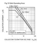
Example of a 1W 60V NPN transistor.

Notice 10ms @40V= 300mA max. . . You can extrapolate down to 10uS and obtain higher currents, which will be limited by beta and Ib and effective ESR of device.

Look at intersection of 40V axis
  • 150mA DC max
  • 200mA @ 100ms max
  • 280mA @ 10ms max

  1. note results are not pure Joule related due to physical heat transfer of this design
  2. More rugged devices will follow VI*t curve
  3. for thermal runaway, thermal resistance, Zθ, must be lower than drop in ESR electrical resistance and Vce Schockly effect at rising ( I and Temp,T)
  4. Zθ*ΔT ≥ |ΔVce/ΔI| =my ESR runaway criteria
image.jpg

When in doubt of max I vs Δt product short circuit limit, choose a part with rated pulse current curves and choose protection time less than max rated time!! i.e. If not rated for 10x nominal current in 10us, it is not reliable.
 

Although I (and erikl) have focused on the physical-thermal limit based on materials, I also alluded to the possibility that you could
see a loss of controllability or runaway at lesser temperatures, which could defeat an active-circuit protection (if the gate does
not control the current, then what you do to it ceases to help).

High temp increases body shunt resistance and improves the parasitic BJT gain, also runs up the on resistance and much of this is in the neck region, which is a small portion of total die area and so heat input is nonuniform (putting the lie to bulk volume based heat capacity calcs, as the real deal for temp rise where it counts).

This all argues for you to blow some stuff up on the bench, to derive your design limits.

A passive limiting resistor is certainly a useful tool, but it would not be tolerable in a path where high-legit-load efficiency is important.

Sometimes (like in bipolar op amps) I have seen the sense resistor for current limiting also serve as a backstop current limiter - not large enough to fully limit the totem pole current to designed value, but perhaps giving you a somewhat longer time at lesser current, to get it together protection-wise.

If you put the resistor in a drain / collector leg, you will see less impact than with a source degeneration, in normal operation.
 
Last edited by a moderator:

Thanks everyone who replied, and most thanks to erikl - that's exactly what I was looking for!
 

Status
Not open for further replies.

Part and Inventory Search

Welcome to EDABoard.com

Sponsor

Back
Top