Hilbertstrauss
Newbie level 5

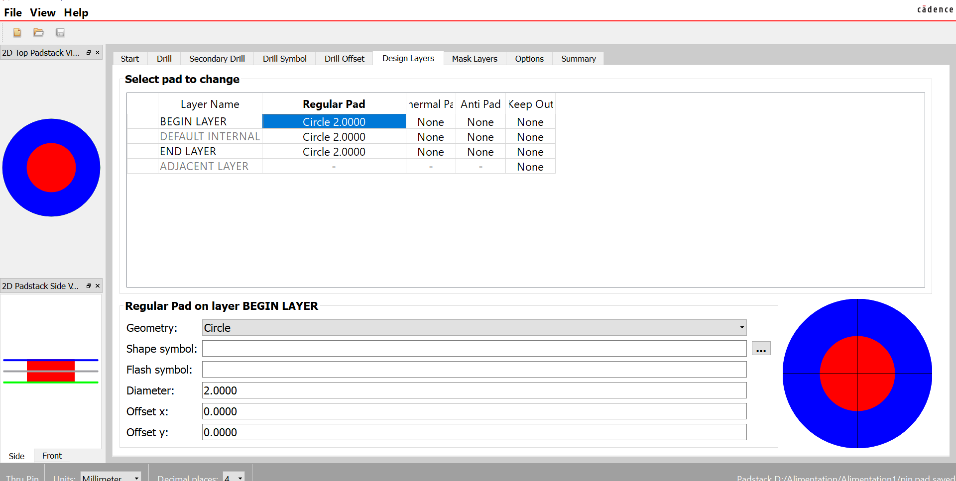
I wanted to create the pad file for a thru-hole pin using pad editor. The hole has a 1mm radius. I set BEGIN LAYER to 2mm.
Is BEGIN LAYER the copper layer adjacent to the hole on the top side of the PCB? And if I set its radius to 2mm would this mean the copper pad ring will have a thickness of 1 mm (assuming, hypothetically, 0 mm tolerance)?

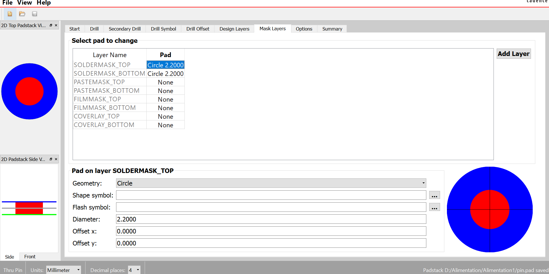
What also confuses me is how the assignment of the radius of SOLDERMASK_TOP layer works. If for example I set it to 2.2 mm would this mean I will have a ring of solder mask between a radius of 2mm and a radius of 2.2mm? But I thought the solder mask was supposed to cover copper surfaces, I'm trully confused about how I should set its radius and what it would actually mean.

Your help would be much appreciated!
Is BEGIN LAYER the copper layer adjacent to the hole on the top side of the PCB? And if I set its radius to 2mm would this mean the copper pad ring will have a thickness of 1 mm (assuming, hypothetically, 0 mm tolerance)?
What also confuses me is how the assignment of the radius of SOLDERMASK_TOP layer works. If for example I set it to 2.2 mm would this mean I will have a ring of solder mask between a radius of 2mm and a radius of 2.2mm? But I thought the solder mask was supposed to cover copper surfaces, I'm trully confused about how I should set its radius and what it would actually mean.
Your help would be much appreciated!
