gaom9
Full Member level 4

Hi,
I am working in a Δ-Σ Fractional-N Frequency Synthesizers, I have a question about the design of output network of it.
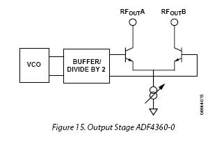
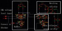
Because the output of the PLL should have a 50Ω matching, so I want to use the Open collector with a off-chip LC network to ensoure the matching as shown in the figure following.


My question is the connection of the output buffer driver to the NPN transistor. I am sorry that I am not familiar with the BJT circuit design, and I do not know how to make a good DC biasing to the NPN.
The input signal of the output network is CML voltage level from 1.1V--1.8V, and this signal is connected to the output network and the divider, in order to ensure this signal not be effected by the NPN transistor, I add a CML buffer between the signal input and the NPN transistor. The gain of this buffer is 1 at the input frequency point, but I find when it is connected to the NPN transistor, the signal will attenuation to be less than 0.2V and distortion. It makes the output signal of the matching network quite little(the output amplitude I want is about 200mV), why?
How can I avoid this? And I try to use the AC capacitor and additional DC bias to between the buffer and the NPN, but it work quit bad.
What should I pay more attention to in designing this type of circuit?
And is there any other type of output network to use as the output network of the PLL?
The frequency range of the SDPLL is 2.4G to 2.6G. And I try to use the MOS replace the NPN, but it works much worst than the NPN.
Thank you.
Best regards!
I am working in a Δ-Σ Fractional-N Frequency Synthesizers, I have a question about the design of output network of it.
Because the output of the PLL should have a 50Ω matching, so I want to use the Open collector with a off-chip LC network to ensoure the matching as shown in the figure following.


My question is the connection of the output buffer driver to the NPN transistor. I am sorry that I am not familiar with the BJT circuit design, and I do not know how to make a good DC biasing to the NPN.
The input signal of the output network is CML voltage level from 1.1V--1.8V, and this signal is connected to the output network and the divider, in order to ensure this signal not be effected by the NPN transistor, I add a CML buffer between the signal input and the NPN transistor. The gain of this buffer is 1 at the input frequency point, but I find when it is connected to the NPN transistor, the signal will attenuation to be less than 0.2V and distortion. It makes the output signal of the matching network quite little(the output amplitude I want is about 200mV), why?
How can I avoid this? And I try to use the AC capacitor and additional DC bias to between the buffer and the NPN, but it work quit bad.
What should I pay more attention to in designing this type of circuit?
And is there any other type of output network to use as the output network of the PLL?
The frequency range of the SDPLL is 2.4G to 2.6G. And I try to use the MOS replace the NPN, but it works much worst than the NPN.
Thank you.
Best regards!
