Continue to Site

Welcome to EDAboard.com

Welcome to our site! EDAboard.com is an international Electronics Discussion Forum focused on EDA software, circuits, schematics, books, theory, papers, asic, pld, 8051, DSP, Network, RF, Analog Design, PCB, Service Manuals... and a whole lot more! To participate you need to register. Registration is free. Click here to register now.

About Chock Inductor?

Status
Not open for further replies.
From watching animated simulations, I have seen a difference in (a) the times when current flows in the secondary, and (b) the direction it flows (or wants to flow). After power-up it does one thing, then after a while it does the opposite, after operation has levelled out to a normal running state.

I think it has something to do with the amount of charge on the output capacitors.

In your circuit, there are two diodes which can carry secondary current (at opposite times of course).
(1) After power-up, one diode is the chief carrier of current. Secondary current flow occurs simultaneously with current flow in the primary.

(2) As operation continues there is a gradual changeover. The other diode becomes the chief carrier. Secondary current flow occurs at a different time than primary current flow.
 

I fear the question is unclear. Do you mean the Lin and Lout current probes? They are showing exactly the same current, with different polarity, by convention.
 

Hello FvM,

Yes, it's exactly same current. But, why its different polarity (or) why its 180 degrees phase shift? Please can you explain clearly?
 

It's how these current probes work. Refer to the software manual.

What do you expect, should they define positive polarity from left to right or downwards? A usual convention is to define current into a device as positive, or vice versa.
 

OK thank you FvM...
 
Last edited:

Last edited:

There's obviously another mechanism that rules Vds, probably the current at the output side. You should observe all circuit currents and voltage to understand what's going on.
 
Last edited:


I don't see where you specifically asked about the series resonant circuit.

My simple point is that the combination of L1 and the MOSFET already achieves a voltage above Vin. The complete resonant converter circuit is more complex of course. To analyze it's behaviour, all components have to be considered.
 

Can you please explain the reason...

1. Why the Drian-Source (Vds) is increasing to high value even when the applied input voltage is 60V?

When the switching device turns off, the coil goes into generator mode.
It creates however high a voltage is necessary in order to cause its current flow to continue.

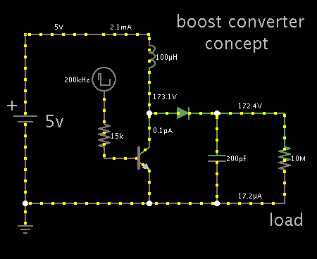
To illustrate the principle, here is a screenshot of a simplified boost converter. It is snapped during switch-Off.

Notice the high volt reading at the lower end of the coil. It needs to rise that high, to overcome whatever is the charge level on the capacitor.

4688048500_1364634882.png
 
1. How & why the Drain-Source voltage (Vds) is achieving a high voltage than the input voltage? and also
2. How & why the Vds is rising to certain high voltage and falling to zero as a half-wave?

Please can you explain clearly by the drawing waveforms step by step then easily understand than the words.

You're in luck. You can watch an animated simulation of my schematic above. It will be more help than words and pictures could ever be.

The simulator is the one at falstad.com/circuit. Click the link below and it will open the website, load my schematic, and run it on your computer.

https://tinyurl.com/bq4gqfl

The speed control is a slider at the right side of the window.
If you slow down the speed while the bias is on, you will see current building in the power loop.

Then when the bias turns off, you will see the high voltage spike generated by the coil.

You can alter values by right-clicking on a component, then selecting Edit.

- - - Updated - - -

1. How & why the Drain-Source voltage (Vds) is achieving a high voltage than the input voltage? and also
2. How & why the Vds is rising to certain high voltage and falling to zero as a half-wave?

Please can you explain clearly by the drawing waveforms step by step then easily understand than the words.

You're in luck. You can watch an animated simulation of my schematic above. It will be more help than words and pictures could ever be.

The simulator is the one at falstad.com/circuit. Click the link below and it will open the website, load my schematic, and run it on your computer.

https://tinyurl.com/bq4gqfl

The speed control is a slider at the right side of the window.
If you slow down the speed while the bias is on, you will see current building in the power loop.

Then when the bias turns off, you will see the high voltage spike generated by the coil.

You can alter values by right-clicking on a component, then selecting Edit.
 
Hello BradtheRad,

What is meaning of generator mode? as you said in post 13..
 
Last edited:

Hello BradtheRad,

What is meaning of generator mode? as you said in post 13..

It's the same as the coil discharging.
The flux field collapses, creating current.

It generates current. It acts like a battery, with a positive and a negative terminal.

I have a Youtube video (or two) which is an animated simulation of coil behavior. It portrays the flux lines building and collapsing. It portrays changing counter-EMF.

Inductor behavior with DC:

https://www.youtube.com/watch?v=LVNxrN4jgvs
 

Last edited:

This converter is a tough one to figure out. It contains both a boost converter, and a flyback converter, and at least one resonating loop.

I have a simulation running. (I guessed at the values of a few unknown parameters.)

I am watching resonant frequencies at: (a) a couple MHz through the supply, and (b) several MHz around a loop containing the transformer primary.

If you drive an LC tank loop at its resonant frequency, the resulting action has the ability take a low voltage supply input, and escalate it to a high voltage waveform.

That is probably what you are seeing. (Although I am not sure what is normal operation in this converter.)
 

Status
Not open for further replies.

Similar threads

Part and Inventory Search

Welcome to EDABoard.com

Sponsor

Back
Top