hugo92
Newbie level 4

Hi , As a project i'm triyng to simulate a TSPC Flip flop that works correct.
I don't know where s the problem that my program works incorrect.
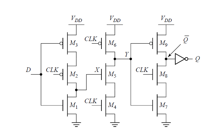
This is the Pos edge TSPC flip flop:
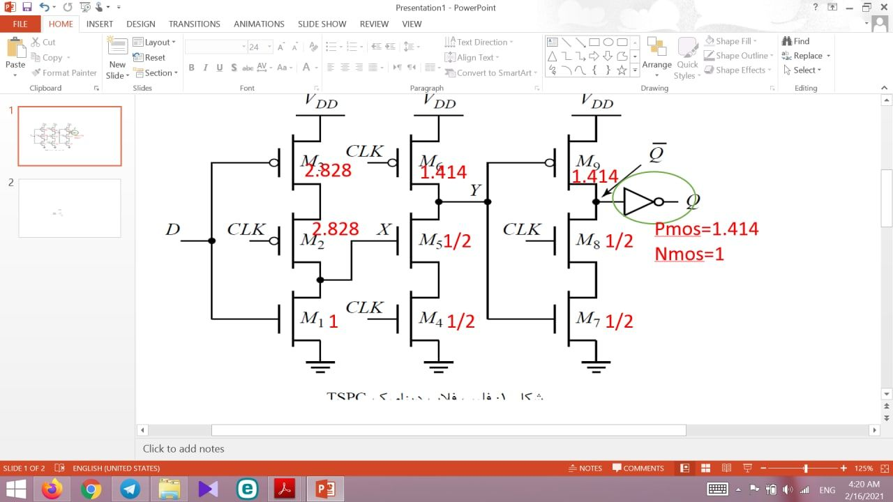
This is sizing I choosed:
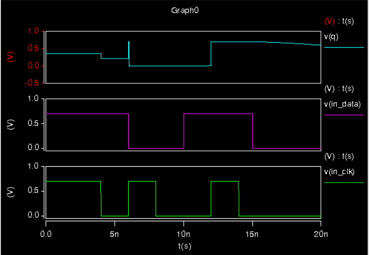
And this is my Hspice simulation waves:
it's obvious that flip flop isn't working fine.
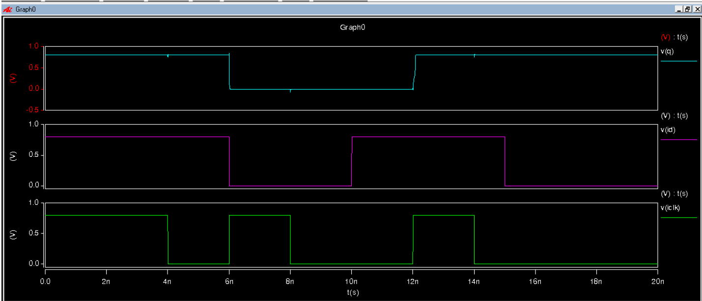
This is a correct flip flop waves working fine which somebody else sent me:
can u please help me .
I think my hspice code is ok , anyway its here:
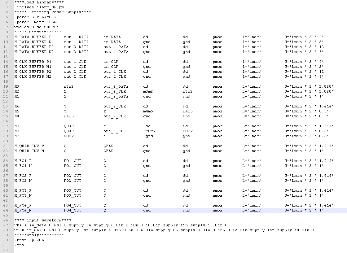
FO1,FO2,FO3,FO4 are 4 inverters as capacitive load in the output node(Q).
and also I used a buffer before input signals in order to have real signals.
I don't know where s the problem that my program works incorrect.
This is the Pos edge TSPC flip flop:
This is sizing I choosed:
And this is my Hspice simulation waves:
it's obvious that flip flop isn't working fine.
This is a correct flip flop waves working fine which somebody else sent me:
can u please help me .
I think my hspice code is ok , anyway its here:
FO1,FO2,FO3,FO4 are 4 inverters as capacitive load in the output node(Q).
and also I used a buffer before input signals in order to have real signals.
