Continue to Site

Welcome to EDAboard.com

Welcome to our site! EDAboard.com is an international Electronics Discussion Forum focused on EDA software, circuits, schematics, books, theory, papers, asic, pld, 8051, DSP, Network, RF, Analog Design, PCB, Service Manuals... and a whole lot more! To participate you need to register. Registration is free. Click here to register now.

A question regarding routing angle in PCB design

Status
Not open for further replies.

venn_ng

Member level 5
Member level 5
Joined
Mar 26, 2017
Messages
87
Helped
1
Reputation
2
Reaction score
1
Trophy points
18
Activity points
645
Hi,

I see that the routings in a PCB don't turn by 90 degrees to avoid the hard discontinuity for the flow of electrons. My question is if that's the case is the following routing (marked in blue) not recommended? Should it be curved?
 
Last edited by a moderator:

Re: A question regarding routing in PCB design

Routing at diagonal angles is a policy actually adopted in PCB designs, but it is only for layout involving signals with an extremely high transfer rate, which does not appear to be the case with the above snapshot, first because it is seeminglly a potentiometer, and also because its track is a little thicker, implying that it is not a data signal connection, but perhaps just biasing.
 

If it is truly high speed then they don't even use any corners, but make the traces curved to keep the width of the trace (hence the impedance) constant.

The issues with 90 bends is that there can be local heating of the trace (if it's supplying power) at the inside corner as more electrons will want to take that path than go near the far outside corner. It also affects the impedance of the trace somewhat due to the larger trace width at the 90 bend. The typical 45 degree bend still causes an impedance discontinuity (it creates two of them too!).
 

Actually, this is a controversial subject; although I particularly do prefer doing corner traces in 45 degrees rather than right angles ( which I use only in the actual edge of the board for thick power nets - just to fill these regions ), there are numerous reports mentioning that in practice it doesn't matters at all even form highest frequencies. The only reason that keeps myself doing this fashion however is that by using 2*45 angles should give a relative better performance than by using a single 90 degree corner. We should agree that a round corner is nothing else than an almost infinite chaining of small angle corner traces ( n*(90/n) ). Another point worthy of attention is that traces at right or diagonal angles (0/45/90) are easiest to draw by plotters, which are made either by moving the x and y step-motors at the same rate or independently, while the other angless would require a rendering that could generate jag of the track, particularly perceptible on fine tracks.
 

We discussed this recently on this thread... Below GHz signals 90 degree corners don't make any difference.
Never heard of localised heating of traces on power designs and I've done some hefty one, I would like to see some citations regarding that, because it sounds like another PCB myth. Impedance, read up, Howard Johnson for one this thread for another.

- - - Updated - - -

Hi,

I see that the routings in a PCB don't turn by 90 degrees to avoid the hard discontinuity for the flow of electrons. My question is if that's the case is the following routing (marked in blue) not recommended? Should it be curved?

I would suggest you look up drift velocity of electrons as a corner IS NOT going to effect the flow of electrons, they only move at about 0.1mm a second, if that...

Curved traces again only when you get into reasonably high GHz signalling, normal stuff doesn't give a dam.

Now we have had a bit of fun with some PCB myths, lets think about this... on EVERY two layer or above board you have numerous signals going through 90 degree bends, high speed, power, analogue and there are never any problems or localised heating, so forget the myths and don't worry about 90 degree corners. And I do mean EVERY board.....


Some facts:

http://www.sigcon.com/Pubs/edn/bigbadbend.htm

http://montrosecompliance.com/wp-content/uploads/2014/09/corners-USA.pdf

Some discussions:
https://www.edaboard.com/threads/343118/
https://www.edaboard.com/threads/349822/

And some fun:
http://www.ultracad.com/articles/flying.htm

The latter from 1996 (21 years ago now...)
 

We discussed this recently on this thread... Below GHz signals 90 degree corners don't make any difference.
Never heard of localised heating of traces on power designs and I've done some hefty one, I would like to see some citations regarding that, because it sounds like another PCB myth. Impedance, read up, Howard Johnson for one this thread for another.

This was from the many power analysis done on various boards done for us. Where we would have to change layout to pass the power analysis due to problems with localized current densities being so high that they would cause problems with the board due to heating and some other issue, which I don't recall, (I'm an FPGA/ASIC guy not a board designer) I think it had to do with reliability of the trace like something to do with metal migration or such, I really don't recall. But these issues were mostly in sections of a design where a wide trace (it wasn't a power plane) was too narrow and there was a 90 bend that then expanded into a much more plane like section that supplied 2 FPGAs and other logic. Basically this corner had severe power density issues on the inside edge of the corner and it was changed to increase the width of the feeder trace (to be more of a plane) and some interfering components were move around to add some copper so the 90 degree bend was removed and one of the FPGAs was not hidden around the corner so much. Regardless maybe it's a myth, but it a myth based on physics...because when you increase current density (localized current) you end up with more heating due to I^2*R loss. Or are you telling me that there is no such thing as I^2*R power loss and every trace can be considered a superconductor 8-O

The trace impedance stuff with curved traces was because the designs the RF guys were working on were in the 10's of GHz range and they had some really hard to meet specs.
 

Read what I said I never mentioned anything about I^2*R or that it doesn't exist...:sad:
In 35 years of doing PCB design, including many high power designs I have never heard of localised heating due to a 90 degree bend or can I find anything covering the issue, but I do have plenty of stuff on high power design and no mention. So I would strongly suspect it was not the 90 degree trace just copper necking down. Why would the corner heat up more... probably more to do with the overall topology of the PCB, and where the heat can dissipate to. Off course you could use something like this...
**broken link removed**
It what we use, the DC current function shows hot spots nicely, just the thing you need for say a 14 layer flexi-rigid for aerospace use.
I stated and posted links that all say below GHz 90 degree corners don't have much effect, GHz and microwave stuff is different and layout is critical. That said I don't actually use 90 degree corners on my signals, I do for power though sometimes...
 

Obviously the current density will be slightly higher at the inner corner of a 90 degree bend. But I expect that it can be ignored in PCB design where copper thermal conductivity balances local overtemperature. May be different for IC metal when you already run a trace near the electromigration limit values.

Mitering 90 degree bends shorts total trace length, that's a sufficient reason for it in a low speed design. Board appearance is another one.
 

Actually despite my previous comments, it is true when you reach the elecronmigration levels corners can be an issue... To be honest if you do a PCB and this becomes an issue (ref attached link for some pretty pictures) then you have more problems to worry about, not least the trace heating up. This problem does seem to be a concern for IC's as FvM has mentioned above.

This document shows the effect, but is related to IC design, for PCB we can ignore the issue, that is if you use the recommended trace widths from IPC-2152... The only person I know who faces these sort of problems outside of IC design works with superconductors and related magnetics, again not every day stuff, more cutting edge physics. For the rest of us the electrons just wiggle about in the wire at about 0.025mm/s...
https://www.ifte.de/mitarbeiter/lienig/date2002.pdf
**broken link removed**
Same with RF and microwave layout, its a specialist area of PCB layout and many non-standard practices have to be followed.
 

HI,

Thank you everybody for your replies. So I needn't worry about 90 degree bend for DC signals (in this case it's actually a power signal)?

- - - Updated - - -

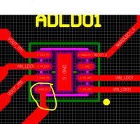
Also, can you tell me if I can connect a routing to a package PAD like this?

Note that it's tilted and doesn't approach horizontally.
 

I would come out of the arc to remove the little nick in the copper and give a smoother line around the copper. Just a little neater and makes etching a little easier. The artwork is expanded slightly during manufacture to cater for etch back, so a smooth polygon shape is prefferable. its a little detail but its these that are important.
 

Attachments

  • eg1.JPG
    eg1.JPG
    31 KB · Views: 175

I would come out of the arc to remove the little nick in the copper and give a smoother line around the copper. Just a little neater and makes etching a little easier. The artwork is expanded slightly during manufacture to cater for etch back, so a smooth polygon shape is prefferable. its a little detail but its these that are important.

Is this ok?
 

Status
Not open for further replies.

Part and Inventory Search

Welcome to EDABoard.com

Sponsor

Back
Top