Continue to Site

Welcome to EDAboard.com

Welcome to our site! EDAboard.com is an international Electronics Discussion Forum focused on EDA software, circuits, schematics, books, theory, papers, asic, pld, 8051, DSP, Network, RF, Analog Design, PCB, Service Manuals... and a whole lot more! To participate you need to register. Registration is free. Click here to register now.

a problem of level shift

Status
Not open for further replies.

gdhp

Advanced Member level 4
Full Member level 1
Joined
Jan 7, 2005
Messages
116
Helped
2
Reputation
4
Reaction score
1
Trophy points
1,298
Activity points
931
hi all

i am designing a circuit. The power is 2.5v, adn the input signal level 2.5v with

25M. I want the output signal level is 1.5v.

can anyone give me some suggestion to perform the function?

Now i have some thought. one is that i use the linear regulator to transfer the 2.5v power to 1.5v.

Another is use the source follower.

some suggestion? some materials?
Thanks!!
 

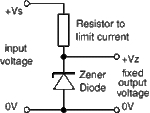
Use a zener diode as a voltage regulator with it's cathode common to the output signal (you wanted to be 1.5V) and a pull-up resistor to your input signal of 2.5V and its anode to the ground.

Another method is to use a buck or step-down converter. It's topology is still source-follower but with added components like inductor, diode and a capacitor.

Simply a source-follower is a common method too. I used that too, in the past for some simple signal conversion.

Linear voltage regulator, most people uses that too.
 

    gdhp

    Points: 2
    Helpful Answer Positive Rating
can you give me some materials?

Added after 1 minutes:

Use a zener diode as a voltage regulator with it's cathode common to the output signal (you wanted to be 1.5V) and a pull-up resistor to your input signal of 2.5V and its anode to the ground.???

i don't understand!can you explain it?
 

Choosing a zener diode and resistor:

The zener voltage Vz is the output voltage required
The input voltage Vs must be a few volts greater than Vz
(this is to allow for small fluctuations in Vs due to ripple)
The maximum current Imax is the output current required plus 10%
The zener power Pz is determined by the maximum current: Pz > Vz × Imax
The resistor resistance: R = (Vs - Vz) / Imax
The resistor power rating: P > (Vs - Vz) × Imax

Example: output voltage required is 5V, output current required is 60mA.
(There is more informaation about regulators on the Electronics in Meccano website. )

Vz = 4.7V (nearest value available)
Vs = 8V (it must be a few volts greater than Vz)
Imax = 66mA (output current plus 10%)
Pz > 4.7V × 66mA = 310mW, choose Pz = 400mW
R = (8V - 4.7V) / 66mA = 0.05k = 50, choose R = 47
Resistor power rating P > (8V - 4.7V) × 66mA = 218mW, choose P = 0.5W
 

Attachments

  • zener_diode_voltage_regulator_119.gif
    zener_diode_voltage_regulator_119.gif
    3.4 KB · Views: 325

    gdhp

    Points: 2
    Helpful Answer Positive Rating
thank you skyhigh!

Another can you give me some suggestions about the source follower. because the output has to connect to 10pf Cap, so the delay-time should be considered .
 

It depends how 10pF capacitor is connected to the source and the load.
 

In the interface between different ligic level application , we often open drain output with a pull up res.

The output with 10pF cap. you can tune the NMOS driver capability and pull up res.
 

i know the opendrain ,but the delay is too large. so i give up it!
 

i am designing a circuit. The power is 2.5v, adn the input signal level 2.5v with

25M. I want the output signal level is 1.5v.

I have questions about ur problem
1. what is 2.5V with 25M ? do u mean 25mV or 25MHz ? input signal level 2.5V is the DC level ?
2. do u have 1.5V power supply ?
3. do ur signal is clock (full swing 0~2.5V), or it is a analog signal ?
4. what's ur load for the 1.5V output ?
5. what application?
 

hi Btrend

1: the input signal is clock signal with full swing of 0- 2.5v, the frequency is 25M.
2: i have no 1.5v POwer. so it is problem.
3:the signal is a clock.
4: the load of output is a PIN, who has a 10pf cap.
5: it is a level shif.
 

level shift from high voltage to low voltage is easy, what u want to do are:
1. produce a 1.5V power supply from 2.5V using LDO like topology
2. cascade two inverters to form a buffer and their VCC connect to 1.5V from (1)
3. 10pF is no problem, if u sizing the final inverter in (2)
 

cascade two inverters to form a buffer ??

why use the cascade two inverters??
 

gdhp said:
cascade two inverters to form a buffer ??

why use the cascade two inverters??
refer to this
 

hi Btrend

thank you for your suggestion! some problems!
1:at the input , the 2.5 dc is divided half and 1.25v is connected to opamp.

2: so i think the output of v15 is 1.5v.

q:
1: why the value of 1.25 is choosed ? can i connect the 2.5 to opamp,and use two resistance to get the 1.5v?

2: at the output ,you use the pmos. i think it is a wrong, it should be nmos. i don't know why couldn't use the pmos??

3:because the ckin is 25M clock, so a current pulse exist on the buffer. so in my simulation, i found the current pulse will change the current on the two resistance. so the output of v15 is not stable. some suggestion to get out of it?
 

u had better read some documents about LDO or regulator to know what I had stated.
such as
 

thank you btrend

i am a fresh man in analog. i will try my best. thank you !
 

Status
Not open for further replies.

Similar threads

Part and Inventory Search

Welcome to EDABoard.com

Sponsor

Back
Top