Continue to Site

Welcome to EDAboard.com

Welcome to our site! EDAboard.com is an international Electronics Discussion Forum focused on EDA software, circuits, schematics, books, theory, papers, asic, pld, 8051, DSP, Network, RF, Analog Design, PCB, Service Manuals... and a whole lot more! To participate you need to register. Registration is free. Click here to register now.

A problem in frabrication: Narrow band filters

Status
Not open for further replies.

hiepsikid007

Newbie level 3
Newbie level 3
Joined
Apr 25, 2012
Messages
4
Helped
0
Reputation
0
Reaction score
0
Trophy points
1,281
Activity points
1,325
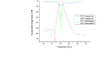
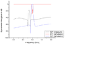
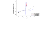
I have simulated some narrow band filters in the CST 2011 and after that, I have my filters fabricated in Ho Chi Minh city. The results are not good enough as you can see in the images below:
Untitled.png
Untitled1.png
Untitled2.png
3 images belong to 3 different filters but they have the same problem, this is:
The characteristics of S21 parameters that are measured in the fabricated filters are bad at the passband.
S21 (measure) must look like S21 (simulation) and also S11 but it's not and I wonder why?
Would you like to give me some advices?
 

You seem to have simulated in CST without loss, because your 0dB passband insertion loss is too ideal to be true. For narrow band filter, it is very important to include metal loss and dielectric loss in the simulation model.

The differences between simulation and measured can be from simulation problems (meshing) and/or tolerances in the hardware (dimensions and material properties).
 
Last edited:

In my opinion before to designa filter you need information about fabrication tolerances, then you can design it giving some attention to them. Take care about the losses
 
I am afraid I cannot agree with upstairs....dielectric/cond. loss won't make a 10dB IL.

R u making Microstrip filters with SMA connectors? Seems like the biggest suspect is your input/output coupling. Make sure you did a good job on soldering at the connectors.
 

    V

    Points: 2
    Helpful Answer Positive Rating
It can. This depends on the filter bandwidth.

in his case, it cannot.

His narrowest BW is around 2%, and filter order less than 5, which is not possible to have 10db level IL, based on current regular dielectric material.
 

    V

    Points: 2
    Helpful Answer Positive Rating
Next time you should add a 50 Ohm 1 Lamda Strip line to your design. From this you will be able to see
what kind of accuracy you have with your Simulation and your integration (SMA's connection/Testing).
 

    V

    Points: 2
    Helpful Answer Positive Rating
From the measured S11 plots, which is about 5-6 dB, the filter is not correctly tuned. Besides, in your measurement, you need better calibration, and better grounding from your measurement connectors.
 

I am afraid I cannot agree with upstairs....dielectric/cond. loss won't make a 10dB IL.

R u making Microstrip filters with SMA connectors? Seems like the biggest suspect is your input/output coupling. Make sure you did a good job on soldering at the connectors.

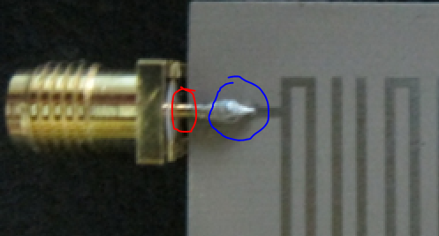
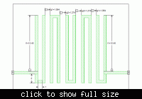
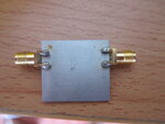
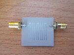
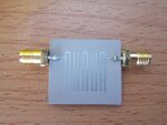
I have the same suspect with u, but I am not sure about how is good job on soldering at the connectors SMA? There are some images of my design and it's results, the real filter is also captured in the following:
2.png3.pngUntitled1.png
Would u like to give me some advices on soldering at the connectors SMA?

- - - Updated - - -

From the measured S11 plots, which is about 5-6 dB, the filter is not correctly tuned. Besides, in your measurement, you need better calibration, and better grounding from your measurement connectors.
Please give me more details when u said "the filter is not correctly tuned"? and also thank so much for your helps!
 

I have the same suspect with u, but I am not sure about how is good job on soldering at the connectors SMA? There are some images of my design and it's results, the real filter is also captured in the following

You have not done a good job, but neither have you used the right sort of SMA connectors. Your ones have round inners, which are deisgned to insert a wire into them, and then. But you can buy them with a strip of metal coming out, which are designed for use on microstrip. You also need to put them against the PCB. We can't see how you have soldered them underneath.

Dave
 
I agree with Dave that this SMA connection is not appropriate.

I want to reproduce the filter simulation. What is the substrate material and thickness?
 

I can't imagine that the SMA connector matching error causes a -20 dB(!) S21 drop, presumed that the SMA ground pins are soldered somehow to the ground plane. There must be a more basic deviation between design and simulation.
 
I can't imagine that the SMA connector matching error causes a -20 dB(!) S21 drop, presumed that the SMA ground pins are soldered somehow to the ground plane. There must be a more basic deviation between design and simulation.


It's likely a combination of many effects:

- The simulation results shown above with 0dB insertion loss must be from lossless simulation.
- Manufacturing tolerances will have an effect. However, there are no critical narrow gaps in the layout.
- The SMA connection has a gap (=inductive) and then a fat solder point (=capacitive).

There might be more problems - we don't know if the simulation was done properly (besides the issue with loss).

49_1345021514.png


- - - Updated - - -

I made an educated guess what the substrate is, because the surface strcuture and pattern looked familiar: Rogers TMM.

So I simulated with TMM6 and TMM10 and found that it seems to be TMM10 indeed. To verify the effect of loss, I simulated the model without loss, and with loss (dielectric loss + conductor loss). For the metal, I also included the surface roughness per Rogers data sheet (1/2 oz copper: 1.8µm bottom and 0.4µm top side RMS roughness). Compared to lossy simulation with smooth metal (not shown), the roughness causes a slight shift in center frequency, and slightly increases the loss.

For the model, I did include some length of feedline, because that is also included in the measurement.

 
Last edited:

If a full engineering drawing, with exact dimensions, substrate material and thickness can be produced I'll have a go in HFSS.
 
  • Like
Reactions: hiepsikid007

    V

    Points: 2
    Helpful Answer Positive Rating

    hiepsikid007

    Points: 2
    Helpful Answer Positive Rating
Did the original poster actually solder the SMA connector to the groundplane? The fact there is a gap between the PCB and the SMA connector is making me wonder if they were actually soldered, or if that gap was intensional to stop the SMA connector shorting to the groundplane. If the response was measured on a network analyzer, the outer conductors would be connected at the analyzer, so the response might not be so far changed.

I'm guessing this is an unlikely possibility, but it would be nice to get it confirmed.
 
I agree with Dave that this SMA connection is not appropriate.

I want to reproduce the filter simulation. What is the substrate material and thickness?

If a full engineering drawing, with exact dimensions, substrate material and thickness can be produced I'll have a go in HFSS.


It's likely a combination of many effects:

- The simulation results shown above with 0dB insertion loss must be from lossless simulation.
- Manufacturing tolerances will have an effect. However, there are no critical narrow gaps in the layout.
- The SMA connection has a gap (=inductive) and then a fat solder point (=capacitive).

There might be more problems - we don't know if the simulation was done properly (besides the issue with loss).

49_1345021514.png


- - - Updated - - -

I made an educated guess what the substrate is, because the surface strcuture and pattern looked familiar: Rogers TMM.

So I simulated with TMM6 and TMM10 and found that it seems to be TMM10 indeed. To verify the effect of loss, I simulated the model without loss, and with loss (dielectric loss + conductor loss). For the metal, I also included the surface roughness per Rogers data sheet (1/2 oz copper: 1.8µm bottom and 0.4µm top side RMS roughness). Compared to lossy simulation with smooth metal (not shown), the roughness causes a slight shift in center frequency, and slightly increases the loss.

For the model, I did include some length of feedline, because that is also included in the measurement.


Did the original poster actually solder the SMA connector to the groundplane? The fact there is a gap between the PCB and the SMA connector is making me wonder if they were actually soldered, or if that gap was intensional to stop the SMA connector shorting to the groundplane. If the response was measured on a network analyzer, the outer conductors would be connected at the analyzer, so the response might not be so far changed.

I'm guessing this is an unlikely possibility, but it would be nice to get it confirmed.

Thank you so much for all your help :D

IMG_4548.JPGIMG_4549.JPG

As you can see, I have already soldered the 2 pins to the ground plane.
I used the substrate TACONIC with the following firgures:
Thickness = 0.635 mm, epsilonr = 10, and the loss tangent = 0.0035 at 2 GHz
The microstrip line is copper with the thickness of 1.75 micrometre
I simulated the filter model in CST MICROWAVE STUDIO 2011 with the mode of Frequency Domain Solver
And about the loss of the substrate, I filled in CST as the following image:
6.png
Is it ok with that loss in the CST STUSIO?
 
Last edited:

As you can see, I have already soldered the 2 pins to the ground plane.
It can't be seen for sure, if the solder is wetting the ground plane or it's possibly a cold solder joint. But I guess, the connector is "soldered somehow", as presumed in post #12.
 

It can't be seen for sure, if the solder is wetting the ground plane or it's possibly a cold solder joint. But I guess, the connector is "soldered somehow", as presumed in post #12.

Sorry for the inconvinience, I post again the images:
IMG_4548.JPGIMG_4549.JPG
 

I was referring to the doubts raised by the bottom photo. A good solder joint would show a concave surface spreading across the ground plane, but it looks more like a drop on top of it. There still may be sufficient electrical connection, but it can't be clearly seen from the photo.
 
I too agree with FvM. It looks to me like the iron used does not have enough heat, as the solder does not seem to have flowed properly.

It might be worth ordering a couple of the right sort of SMA sockets, and removing these, and resoldering on new sockets.
 
Status
Not open for further replies.

Similar threads

Part and Inventory Search

Welcome to EDABoard.com

Sponsor

Back
Top