Continue to Site

Welcome to EDAboard.com

Welcome to our site! EDAboard.com is an international Electronics Discussion Forum focused on EDA software, circuits, schematics, books, theory, papers, asic, pld, 8051, DSP, Network, RF, Analog Design, PCB, Service Manuals... and a whole lot more! To participate you need to register. Registration is free. Click here to register now.

A 3-stage can work correctly but 4-stage ring vco can't work

Status
Not open for further replies.

qwe221133

Newbie
Newbie level 2
Joined
Aug 16, 2022
Messages
2
Helped
0
Reputation
0
Reaction score
0
Trophy points
1
Activity points
17
Hi,
i need to design a CDR so i want to design a 4-stage ring oscillator for my phase detector,my stage schematic is in the picture below, i use hspice to simulate this VCO,i found that when i use 3-stage , VCO works,but in 4-stage it can't be oscillate,it's so weird!! I am pretty sure the circuit connected correctly, does anybody know the reason why 4-stage VCO can't oscillate?

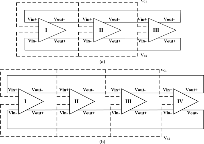
1660632189470.png
1660632161278.png
 

If you have an even number of stages, the circuit has two stable states, so it will settle in one of them.
You must have an odd number of stages.
 
If you have an even number of stages, the circuit has two stable states, so it will settle in one of them.
You must have an odd number of stages.
But my schematic of VCO is fully differential,and i have seen some papers that discuss about even numer of stage,and all of them can work in even stage, i just dont know why my circuit cant work,i put my circuit below.

Code:
x1 VDD VSS OUTN4 OUTP4 OUTP1 OUTN1 VCTL DelayCell
x2 VDD VSS OUTN1 OUTP1 OUTP2 OUTN2 VCTL DelayCell
x3 VDD VSS OUTN2 OUTP2 OUTP3 OUTN3 VCTL DelayCell
x4 VDD VSS OUTP3 OUTN3 OUTP4 OUTN4 VCTL DelayCell

.SUBCKT DelayCell VDD VSS INP INN OUTP OUTN VCTL
M1 OUTN INP N1 VDD P_18 W=30U L=0.2U M=1
M2 OUTN INP VSS VSS N_18 W=22U L=0.2U M=1
M3 OUTP INN N1 VDD P_18 W=30U L=0.2U M=1
M4 OUTP INN VSS VSS N_18 W=22U L=0.2U M=1
M5 OUTN OUTP N2 VSS N_18 W=1U L=0.2U M=1
M6 OUTP OUTN N3 VSS N_18 W=1U L=0.2U M=1
M7 N1 VCTL VDD VDD P_18 W=30U L=0.2U M=1
CC1 N2 VSS 0.1P
CC2 N3 VSS 0.1P
.ENDS DelayCell
VVDD VDD VSS 1.8V
VVSS VSS GND 0V
VVCTRL VCTRL VSS 0.9V
.OP
.TRAN 0.1N 0.5u
.PROBE V(*)

.IC V(OUTP4 )=0.4V
 
Last edited by a moderator:

Ok, with differential stages it should work with an even number if the connections are correct.
I can't see the problem in the code.
 

Hi,

Too complicated for me. Not familiar with differential ring oscillators at all. However, have you considered a start-up helper circuit, to ensure it always starts the same way? Do any of the documents you've read mention expectable start-up behaviour or at transistor level, show anything like e.g. a MOS used as a start-up capacitor?
 

Status
Not open for further replies.

Part and Inventory Search

Welcome to EDABoard.com

Sponsor

Back
Top