Continue to Site

Welcome to EDAboard.com

Welcome to our site! EDAboard.com is an international Electronics Discussion Forum focused on EDA software, circuits, schematics, books, theory, papers, asic, pld, 8051, DSP, Network, RF, Analog Design, PCB, Service Manuals... and a whole lot more! To participate you need to register. Registration is free. Click here to register now.

[SOLVED] 60% mismatch of current mirror, SOS!

Status
Not open for further replies.

lei6042

Newbie level 5
Newbie level 5
Joined
Nov 2, 2009
Messages
8
Helped
0
Reputation
0
Reaction score
0
Trophy points
1,281
Location
china
Activity points
1,354
hi,all
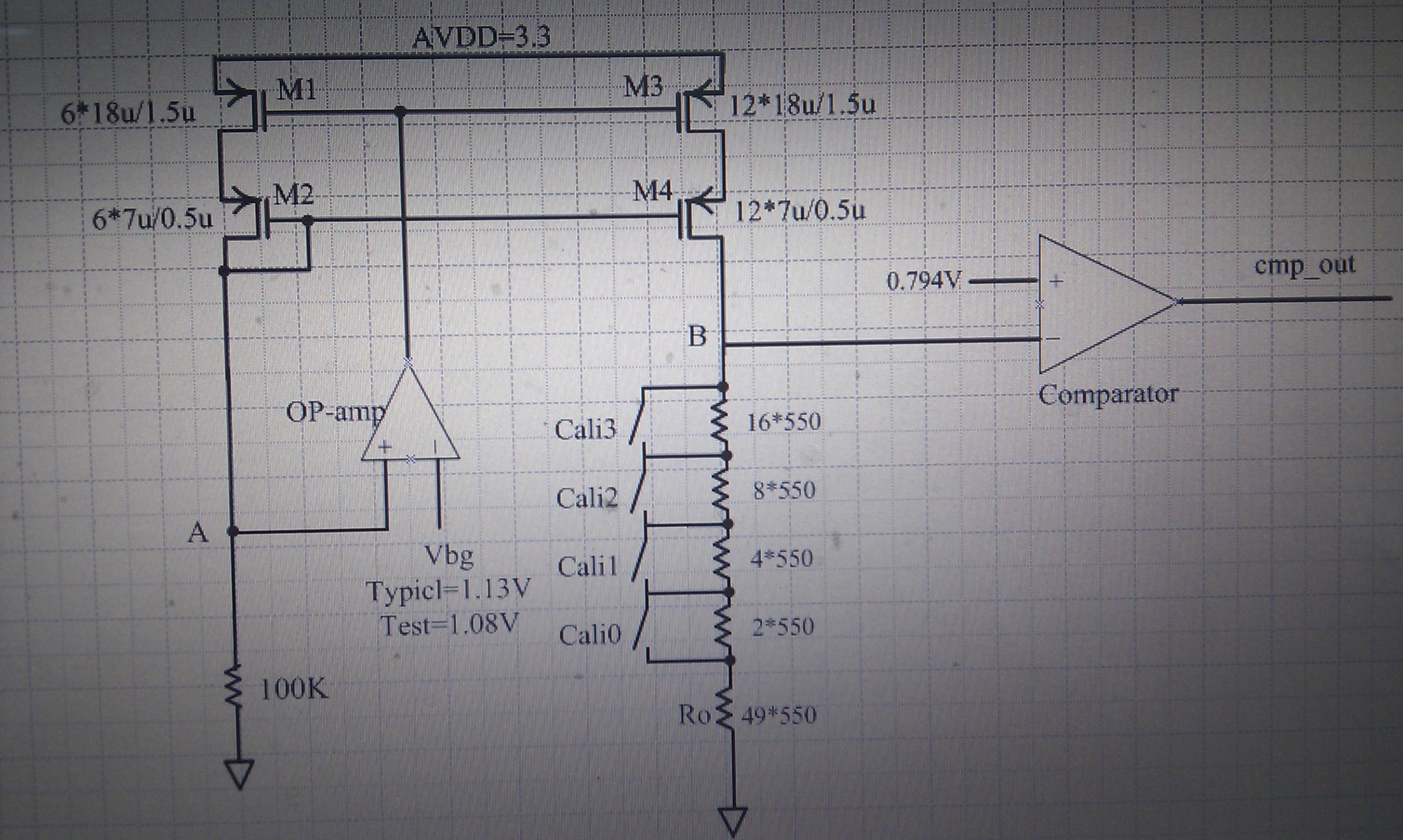
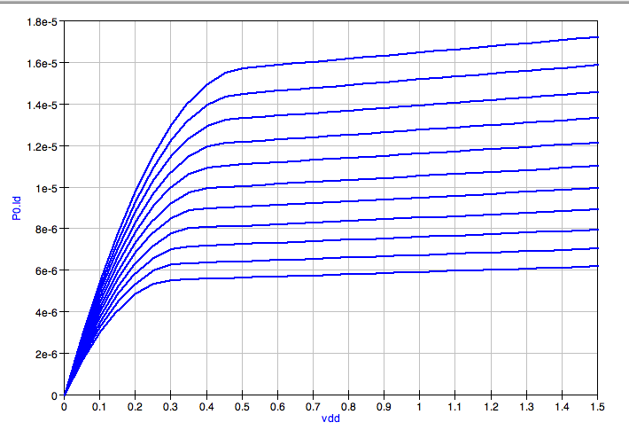
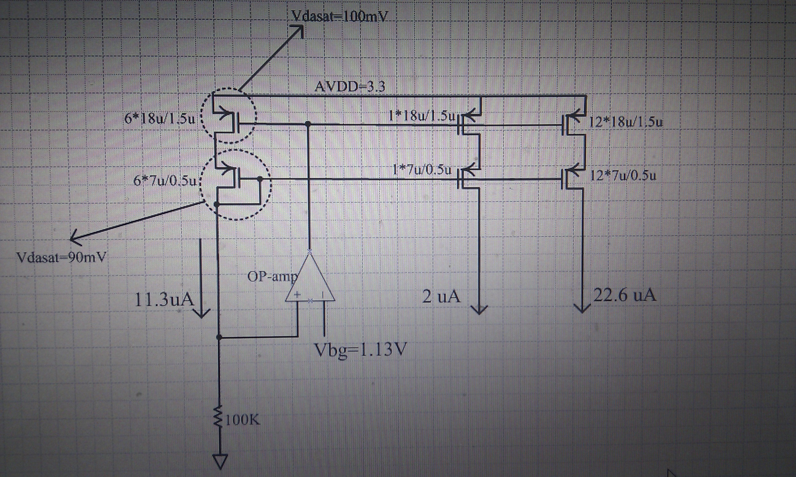
I deigned a group of current mirrors with current ratio of 6:1:12.
That is achieved by pmos ratio of 6*18u/1.5u : 1*18u/1.5u : 12*18u/1.5u.
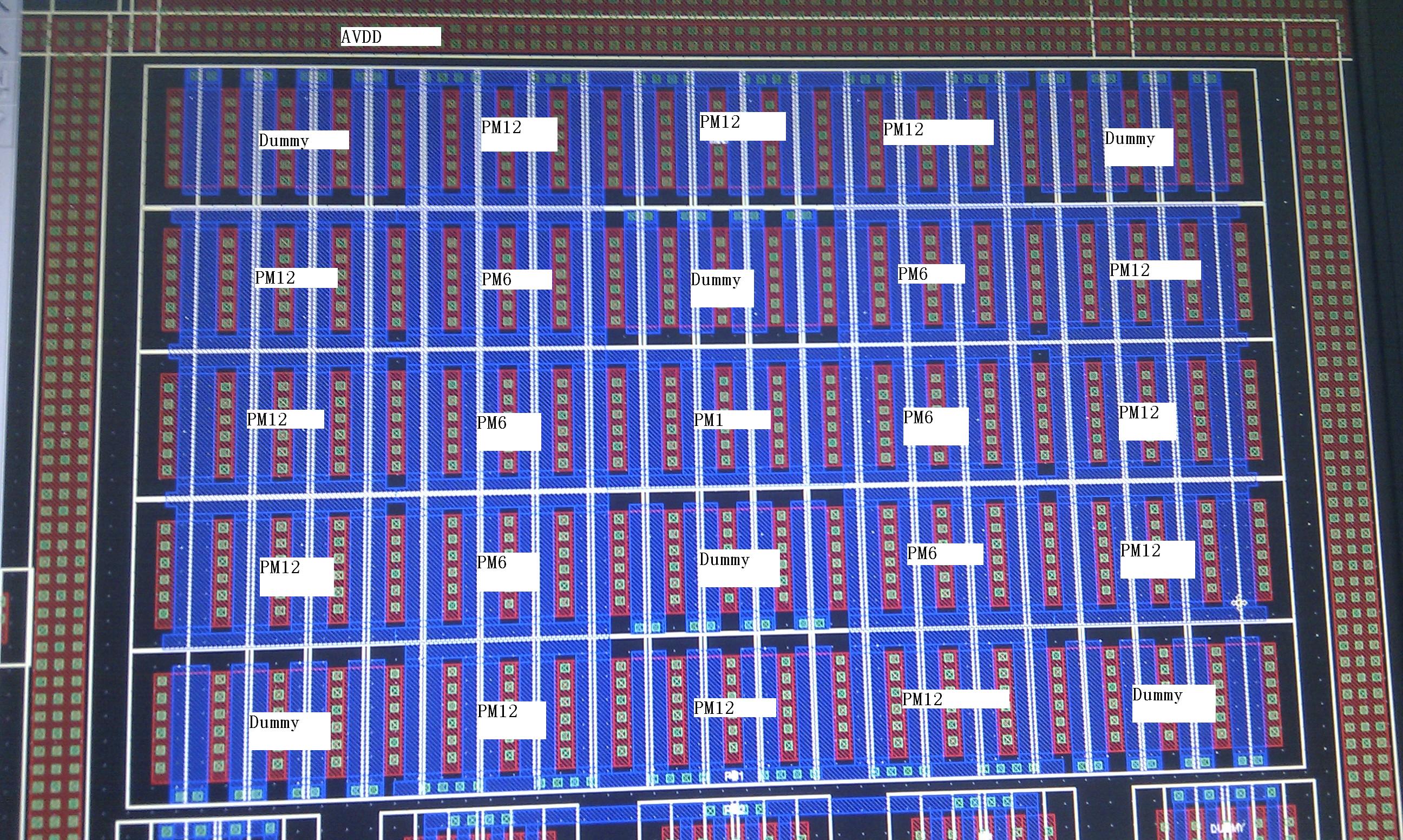
For better matching, I use centroid layout:
Pick the 1*18u/1.5u PMOS (PM1)as "cell" and put it in the center, outside which is the 6 cells (PM6).
Then the 12 cells (PM12) is around PM1 and PM6. Just as the attached pic shows!
Surperisingly, test results shows a 60% mismatch of current. I fail to find the cause of this huge error.
BTW, vdast of the PMOS's is about 100mV. For current matching,that is not a ideal value.
But how can it be so far away from the original desin?
Anyone here has idea about that? Thanks a lot ahead of time!


You didn't tell us your unit current nor your process size. If your VDS,sat is really about 100mV, your PMOS must operate in deep weak inversion mode and your unit current should be around 1µA -- in this case a 60% error seems unbelievable, see here:


But if your unit current is an order of magnitude larger (about 10µA), your MOSFETs operate already in moderate inversion mode, VDS,sat is in the order of 300..500mV, and you could easily get an error of 60% or more between VDS=0.1V and VDS=1V , see here:
 
Hi,erikl
Thanks for your reply.
I upload the schematic figure of my design! The unit current is 2uA and vdsat is 100mV which definitely meets the first case you mentioned
above! The process is UMC 0.35um mixmode.Besides, I used cascode configration to avoid channel-length-modulation effect. So there should be
no big mismatch caused by VDS difference!
I did post simulation of full corner and made sure that the systematic mismatch was whtin an acceptable range!! Now the unacceptable error
drives me to focus on random mismatch caused by layout!
Hope the addtional information helps!
Thanks!


drives me to focus on random mismatch caused by layout!
 

A few possible causes.
1. What resistor are you using? If non-external, you have to cater for +/-20% process variations.
2. How did you measure your output current?
3. The unit current is NOT 2uA. It's more like 1.883333333uA.
4. They way you biased your cascode transistors, they need quite a lot of headroom. What is your output voltage?
5. Is the mismatch only on one part, or all parts? ie systematic or random?

hi,checkmate
answer of your question
1. The 100K resister is external one with high accuracy.Namely the non-inverting input of the op-amp connects to the pin for external resistor
2. We didn't measure the current! We judge the current mismatch by dedution.
3. You are right. mine is just rough estimation.
4. Due to the small vdsat. the headroom seems not be a problem. With output voltage <2V, VDS1+VDS2>1.3V. that is adequate for saturation.
5. May be that is what i am here for answer.:)

thanks!
 

hi,checkmate
answer of your question
1. The 100K resister is external one with high accuracy.Namely the non-inverting input of the op-amp connects to the pin for external resistor
If so, measure the voltage across the resistor. Do you see 1.13V?
2. We didn't measure the current! We judge the current mismatch by dedution.
Mind sharing how the current mismatch was "deduced"?
3. You are right. mine is just rough estimation.
4. Due to the small vdsat. the headroom seems not be a problem. With output voltage <2V, VDS1+VDS2>1.3V. that is adequate for saturation.
The output voltage needs to be lower than 1.13V+Vsg(cascode)-Vdsat(csacode). "<2V output voltage" does not seem convincingly adequate.
5. May be that is what i am here for answer.:)
You have the silicon. Get your hands dirty and start doing measurements!

thanks!
As above ............
 

hi,checkmate
I measured the node voltage of A and got 1.08V(50mv difference from
1.13v due to process variation?!). So I think this curcuit's operating point
is right. The "Output voltage" I mentioned is node voltage of B .
It seems the "Output voltage" you mentioned is node voltage of A.
Also the huge error just happened here because the other part of the chip
works well!

Whatever, I'll show you more details and hope for ur continual concern about my question.
As the pic attached shows, this circuit was designed as caliberation of internal resistor
via external accurate resistor! Vbg/100K generates a reference current which is then
mirrored(2X) and applied to the internal resistors(16*550~49*550). Cali3~Cali0 changes
from 0000 to 1111 (0: swith off. 1: swith on)and generates different voltages with equal
steps. All this voltages are compared with a dc level 0.794V. The Cali3~Cali0 value which
makes comparator output tansfered will be recorded as the final option, thus we
get the calibed-internal-resistance we need.

Now the deduction:
We got the WAT data from fab and find the sheet resistance is 456=550*83%, which
is nearly the max variation to negetive side.Accroding to the design above. Cali3~Cali0
has to be within 0000~0010H (lower part of the code range). But we read 1111 though
LA. We have eliminlate the possibility of code read-out error. So what left is the current
mirror mismatch. Do you think the deduction is reasonalbe? if yes, I haven't found
vonvinced reason to the 60% mismatch.
Hope it helps &Thanks


hi,checkmate
I measured the node voltage of A and got 1.08V(50mv difference from
1.13v due to process variation?!). So I think this curcuit's operating point
is right.
50mV error is on the very high side. I would assume either the bandgap is poorly designed or the opamp has a huge offset.
The "Output voltage" I mentioned is node voltage of B .
It seems the "Output voltage" you mentioned is node voltage of A.
Actually, I was referring to node B. But since it's calibrated to 0.743V, you should not have a headroom issue.
Also the huge error just happened here because the other part of the chip
works well!

Whatever, I'll show you more details and hope for ur continual concern about my question.
As the pic attached shows, this circuit was designed as caliberation of internal resistor
via external accurate resistor! Vbg/100K generates a reference current which is then
mirrored(2X) and applied to the internal resistors(16*550~49*550). Cali3~Cali0 changes
from 0000 to 1111 (0: swith off. 1: swith on)and generates different voltages with equal
steps. All this voltages are compared with a dc level 0.794V. The Cali3~Cali0 value which
makes comparator output tansfered will be recorded as the final option, thus we
get the calibed-internal-resistance we need.

Now the deduction:
We got the WAT data from fab and find the sheet resistance is 456=550*83%, which
is nearly the max variation to negetive side.Accroding to the design above. Cali3~Cali0
has to be within 0000~0010H (lower part of the code range). But we read 1111 though
LA. We have eliminlate the possibility of code read-out error. So what left is the current
mirror mismatch. Do you think the deduction is reasonalbe? if yes, I haven't found
vonvinced reason to the 60% mismatch.
Hope it helps &Thanks

Do you have access to the vbg and 0.743V? You may want to check if their levels are correct.
If you can read the comparator output, you can also verify the trip point and comparator functionality by varying your 100k.
And lastly, check your calibration algorithm to see if you got it right.
Current mismatch may not be the only cause for circuit malfunction.


Thanks a lot for your suggestion! I will try.
 

Status
Not open for further replies.

Part and Inventory Search

Welcome to EDABoard.com

Sponsor

Back
Top